|
市場調査レポート
商品コード
1685905
半導体パッケージング:市場シェア分析、産業動向・統計、成長予測(2025年~2030年)Semiconductor Packaging - Market Share Analysis, Industry Trends & Statistics, Growth Forecasts (2025 - 2030) |
||||||
カスタマイズ可能
適宜更新あり
|
|||||||

| 半導体パッケージング:市場シェア分析、産業動向・統計、成長予測(2025年~2030年) |
|
出版日: 2025年03月18日
発行: Mordor Intelligence
ページ情報: 英文 169 Pages
納期: 2~3営業日
|

- 全表示
- 概要
- 目次
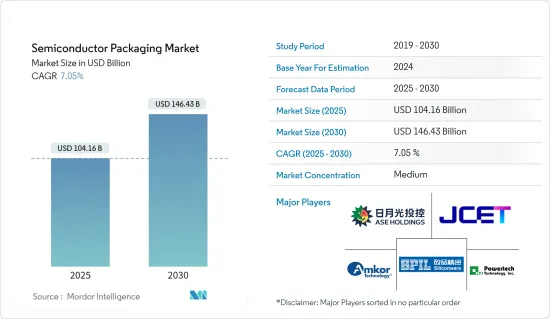
半導体パッケージングの市場規模は、2025年に1,041億6,000万米ドルと推定され、予測期間(2025~2030年)のCAGRは7.05%で、2030年には1,464億3,000万米ドルに達すると予測されます。
半導体パッケージングとは、プラスチック、セラミック、金属、ガラスでできた1つまたは複数のディスクリート半導体デバイスや集積回路を収納するケーシングのことです。パッケージングは、高周波ノイズ放射、静電気放電、機械的損傷、冷却から電子システムを保護するために極めて重要です。
高性能コンピューティング、データセンター・ネットワーキング、自律走行車が、この市場の採用率を押し上げ、技術進化を加速させています。クラウド、エッジ・コンピューティング、デバイスの各レベルで、より巨大なコンピューティング・リソースを持つことが動向となっています。また、通信業界やインフラ業界におけるハイエンド・パフォーマンス・アプリケーションや人工知能(AI)の成長も、調査対象市場の進歩を可能にしています。
フロントエンドノードの小型化に伴い、設計コストの重要性が増しています。先進パッケージング(AP)ソリューションは、システム性能を高めながらコストを削減し、低遅延、帯域幅の拡大、電力効率を提供することで、こうした問題の解決を支援します。
職場のデジタル化の進展、リモートワークや遠隔操作の動向の出現、電子機器に対する消費者の嗜好の高まりにより、幅広い新たな機会を引き出すことができる半導体デバイスへの需要が高まっています。半導体デバイスの成長が加速し続ける中、先進パッケージング技術はデジタル化時代に必要なサイズと処理能力を提供します。
世界各国政府は、障壁を引き下げ、生産、研究開発への補助を強化することで、半導体産業への支援を強めています。例えば、韓国は世界最大のチップセンターを建設するために4,560億米ドルという途方もない民間投資を行い、業界の覇権を握るという野心を強調しています。
これと並行して、韓国政府は半導体産業に対する広範な支援策を展開し、その規模は26兆ウォン(約191億米ドル)に達しました。このプログラムは、金融支援、インフラ開発、R&D、中小企業への的を絞った支援に及んでいます。韓国は現在、ソウル郊外に「メガチップクラスター」を建設中で、世界最大の半導体ハブになると予想され、多数の新規雇用機会を創出する重要な原動力となっています。
自動車、家電、ヘルスケア、IT・通信、航空宇宙・防衛など、さまざまな産業の要求に応じた半導体パッケージング装置の設計、開発、設置には、かなり高額な初期投資が必要となります。これは半導体パッケージング市場の成長を制限する可能性があります。
さらに、各国の国防予算は、インフレ、経済成長、政府支出の優先順位、世界貿易や地政学的力学などの主要なマクロ経済要因に大きく影響されます。
2023年3月、ジョー・バイデン(Joe Biden)大統領は、総額8,860億米ドルの平時最大の米国国防予算を提案しました。この予算には、兵士の給与を5.2%引き上げ、研究開発に過去最高の予算を計上することが盛り込まれました。ウクライナにおけるロシアの行動を背景に、軍需品への支出増の必要性がさらに強調されました。
米国議会予算局によれば、米国は国防費の一貫した増加を目の当たりにすることになり、その予測は2033年まで続きます。2023年、米国は国防費に7,460億米ドルを支出し、2033年には1兆1,000億米ドルに増加すると予測されています。
半導体パッケージング市場の動向
通信・電気通信セグメントがエンドユーザーとして急成長
- ネットワーキングとコネクティビティの進化は目に見えています。有線インフラを通じた音声や視覚信号の基本的なやり取りから、無線インフラを通じてマルチメディアや大量のデータをやり取りする現状へと進化しています。
- 半導体は通信インフラにおいて極めて重要であり、データのキャプチャやエンコードから暗号化、トランスミッション、そして最終的にはユーザーへのプレゼンテーションに至るまで、さまざまなタスクを処理しています。5Gテクノロジーは、IT・通信ネットワークとデバイスの大きな飛躍を予兆するものであり、従来よりも格段に速い速度を提供し、極めて重要な点として、極めて低い待ち時間を誇る。この待ち時間の短縮は、クラウドゲームやVRコンテンツストリーミングのようなアプリケーションには特に不可欠です。このように、通信・通信業界における半導体需要の増加は、半導体パッケージング市場の成長を促進すると予想されます。
- 同様に、米国政府は2024年2月、米国内のワイヤレス技術革新の促進に向けて4,200万米ドルを割り当てた。この資金は、米国の通信事業者、海外の通信事業者、一流大学、機器サプライヤーが参加する共同プロジェクトに充てられました。このイニシアチブは、ダラス・テクノロジー・コリドーに試験・評価・研究開発センターを設置し、ワシントンDCにサテライト施設を設置することを目的としています。これらの施設の主な焦点は、ネットワーク性能のテスト、相互運用性の確保、セキュリティ対策の強化、新しいテスト手法の調査の指揮を執ることです。
- 同様に2023年4月、エリクソンはカナダ政府と協力し、5年間で4億7,000万カナダドル(3億4,544万米ドル)を投資する意向を表明しました。この投資は、6G、5Gアドバンスト、人工知能、クラウドRAN、コアネットワークなどの技術の研究開発に向けられました。このイニシアチブの目的は、この地域の通信産業の成長を促進し、研究施設の開発を支援することでした。このような投資は、通信産業で広く使用されている半導体デバイスの需要を急増させ、市場の成長をさらに後押しすることになります。
- 2024年、新興国の通信業界は、技術的進歩と戦略的市場開拓の混在を見せた。革新的で先進的な半導体ソリューションを取り入れることは、このシフトにおいて重要な役割を果たし、接続性と速度に対するニーズの高まりに応え、セキュリティ、持続可能性、カスタマイズされたユーザー体験などの重要な要素に対応します。進行中の進歩に伴い、電気通信と半導体技術のコラボレーションは、世界のデジタルランドスケープに大きな影響を与えると予想されます。
- クラウド技術の採用拡大、データセンターの普及拡大、5G技術の人気上昇は、半導体パッケージ市場の成長をさらに後押ししています。データセンターとクラウド市場の世界の拡大がデータストレージの需要を煽り、市場の成長をさらに促進すると予想されます。例えば、Cloudsceneによると、2024年3月現在、米国には5,381のデータセンターがあり、これは世界のどの国よりも多いです。
台湾が大きな市場シェアを占める見込み
- 台湾には、TSMC(台湾積体電路製造)やUMC(ユナイテッド・マイクロエレクトロニクス)といった大手半導体メーカーがあります。これらの企業の強固な存在が、先進パッケージング・ソリューションに対する需要を生み出しています。
- 例えば、2024年3月、TSMCはAIチップの需要急増を考慮し、台湾北部、中部、南部で大規模な拡張を開始しました。この拡張には、2ナノメートル工場と最先端のパッケージング工場の導入が含まれます。TSMCは、台湾で今後登場する1ナノメートル技術をサポートするため、8~10カ所の施設に投資する必要性がある可能性さえ示唆していました。
- AIチップの需要の高まりは、CoWoS(Chip-on-Wafer-on-Substrate)などの先進パッケージング技術の必要性を煽っています。この需要の高まりに対応するため、TSMCは台湾のサイエンスパークの中心に位置する竹南で先進パッケージング施設を増強しています。同社は今年、ツールインと生産ラインの統合を開始する予定です。さらに、嘉義にも先進パッケージング施設の建設が今年開始される予定です。
- 顧客のニーズを満たし、ハイパフォーマンスコンピューティング(HPC)、人工知能(AI)、モバイルアプリケーションなどの製品をサポートする台湾のデジタル経済の成長は、半導体チップの小型化・高性能アプリケーションのために半導体ダイを重ね合わせて使用する台湾の半導体パッケージング市場に機会をもたらしています。GSMAの予測では、2025年までに世界のモバイル・インターネット接続の50%以上が台湾の5G技術によって供給されます。
- 例えば、2023年5月、受託チップメーカーである台湾積体電路製造(TSMC)は、世界な競争力を強化するため、2024年に7つの新施設を建設する計画を発表しました。これらの施設には、3つのウエハー工場、台湾の2つのパッケージング工場、海外の2つのウエハー工場が含まれます。この拡張は、高性能コンピューティング・デバイスやスマートフォンに対する世界の需要への戦略的対応です。先進パッケージング工場は2023年に台湾中部で着工しました。
- さらに、嘉義の施設は今年後半に稼動を開始する予定で、2026年までにCoWoS(Chip-on-Wafer-on-Substrate)とSoIC(Small Outline Integrated Circuit)技術を展開する計画です。2024年6月、台湾の半導体企業TSMCは、その先端技術に対する需要の高騰に直面しました。アップルやエヌビディアのような主要企業はTSMCの生産を完全に予約し、注文は2026年まで伸びています。
- この高騰を受け、TSMCは3nmの価格を5%引き上げることを視野に入れているが、先進パッケージングの価格は来年、10%から20%とさらに急騰する可能性があります。TSMCの3nmラインアップは、N3、N3E、N3Pと、新たに加わったN3X、N3Aで構成されています。オリジナルのN3テクノロジーは改良が加えられているが、前年の第4四半期に量産を開始したN3Eは、AIアクセラレータ、プレミアムスマートフォン、データセンター向けに設計されています。
- 半導体は、ヘルスケア産業におけるツールや機器として様々な形で使用されています。超音波技術の利用拡大が同国での半導体パッケージの利用を後押ししており、これは同国の病院におけるヘルスケアデジタル化と電子機器利用の拡大に沿ったものです。台湾では、メーカーは多国籍企業向けの受託製造を通じて、中低価格帯の医療機器の生産と輸出に大きく注力しています。
- 2024年1月、国際貿易局は台湾経済部のデータから、台湾の医療機器生産の急増を強調しました。同省は、2023年の国内総生産額が892万8,333米ドルに達したと発表しており、一貫した上昇傾向を示し、市場の有望な成長軌道を示しています。
半導体パッケージ市場の概要
半導体パッケージング市場は、ASE Technology Holding、Amkor Technology、Jiangsu Changjiang, Electronics Technology(JCET)、Siliconware Precision Industries、Powertech Technology Inc.などの主要企業が存在し、半固体化しています。同市場のプレーヤーは、製品ラインナップを強化し、持続可能な競争優位性を獲得するために、提携や買収などの戦略を採用しています。
- 2024年4月、サムスンのAVPチームはエヌビディアのAIチップ向け先進パッケージングを受注し、将来の広帯域メモリーチップの供給を可能にしました。サムスン電子のAVPチームは、NVIDIAのAIプロセッサーをパッケージングするためのインターポーザーと2.5Dパッケージング技術の提供を担当します。しかし、これらのプロセッサーに使用されるHBMとGPUチップは他のサプライヤーから供給されます。2.5Dパッケージング技術は、インターポーザー上にCPU、GPU、HBMなどのチップを水平に統合することを可能にします。
- 2023年12月、JCETは江蘇省江陰市に半導体パッケージング・テスト博物館を開館しました。同博物館は、集積回路のパッケージングとテストの領域を展示する専門施設です。これは、パッケージングとテスト業界を推進するためのJCETによる新たな試みを意味します。同博物館は、江陰市におけるIC分野の科学技術育成のシンボルであると同時に、パッケージング・テスト業界の業績を紹介するプラットフォームとしての役割も担っています。
その他の特典
- エクセル形式の市場予測(ME)シート
- 3ヶ月間のアナリストサポート
目次
第1章 イントロダクション
- 調査の前提条件と市場定義
- 調査範囲
第2章 調査手法
第3章 エグゼクティブサマリー
第4章 市場洞察
- 市場概要
- 業界の魅力度-ポーターのファイブフォース分析
- 供給企業の交渉力
- 買い手の交渉力
- 新規参入業者の脅威
- 代替品の脅威
- 競争企業間の敵対関係
- 業界バリューチェーン分析
- COVID-19の副作用とその他のマクロ経済要因が市場に与える影響
第5章 市場力学
- 市場促進要因
- 各業界における半導体デバイスの消費拡大
- 新興諸国における有利な政府規制と政策
- 市場抑制要因
- 高い初期投資と半導体IC設計の複雑化
第6章 市場セグメンテーション
- パッケージングプラットフォーム別
- アドバンストパッケージング
- フリップチップ
- SIP
- 2.5D/3D
- 組み込みダイ
- ファンイン・ウエハーレベル・パッケージング(FI-WLP)
- ファンアウト・ウエハーレベル・パッケージング(FO-WLP)
- 従来のパッケージング
- アドバンストパッケージング
- エンドユーザー産業別
- コンシューマー・エレクトロニクス
- 航空宇宙・防衛
- 医療機器
- 通信・電気通信
- 自動車産業
- エネルギー・照明
- 地域別
- 米国
- 中国
- 台湾
- 韓国
- 日本
- 欧州
- ラテンアメリカ
- 中東・アフリカ
第7章 競合情勢
- 企業プロファイル
- ASE Technology Holding Co. Ltd
- Amkor Technology
- Jiangsu Changjiang Electronics Technology Co. Ltd(JCET)
- Siliconware Precision Industries Co. Ltd
- Powertech Technology Inc.
- Tianshui Huatian Technology Co. Ltd
- Fujitsu Semiconductor Ltd
- UTAC Holdings Ltd
- Chipmos Technologies Inc.
- Chipbond Technology Corporation
- Intel Corporation
- Samsung Electronics Co. Ltd
- Unisem(M)Berhad
- Interconnect Systems Inc.(ISI)
第8章 投資分析
第9章 市場の将来
The Semiconductor Packaging Market size is estimated at USD 104.16 billion in 2025, and is expected to reach USD 146.43 billion by 2030, at a CAGR of 7.05% during the forecast period (2025-2030).
Semiconductor packaging refers to a casing that contains one or more discrete semiconductor devices or integrated circuits made up of plastic, ceramic, metal, or glass casing. Packaging is crucial for protecting an electronic system from radio frequency noise emission, electrostatic discharge, mechanical damage, and cooling.
High-performance computing, data center networking, and autonomous vehicles are pushing the adoption rates for the market studied and accelerating its technological evolution. The trend is to have more enormous computing resources at the cloud, edge computing, and device levels. The advancements in the market studied are also possible due to the growth in high-end performance applications and artificial intelligence (AI) in the telecom and infrastructure industry.
As the front-end node becomes smaller, design cost becomes increasingly important. Advanced packaging (AP) solutions aid in solving these problems by reducing the cost while enhancing system performance and offering lower latency, increased bandwidth, and power efficiency.
The increasing digitization of the workplace, the emergence of remote working and remote operation trends, and the growing consumer preference for electronics have increased the demand for semiconductor devices capable of unlocking a wide range of new opportunities. As the growth of semiconductor devices continues to accelerate, advanced packaging technologies provide the size and processing power necessary for the digitized era.
Global governments are increasingly supporting the semiconductor industry by lowering barriers and ramping up production, research, and development subsidies. For instance, South Korea committed a staggering USD 456 billion in private investments to construct the world's largest chip center, underlining its ambitions for industry dominance.
In tandem with this, the South Korean government rolled out an extensive support initiative for its semiconductor industry, valued at KRW 26 trillion (approximately USD 19.1 billion). This program spans financial aid, infrastructure development, R&D, and targeted assistance for its SMEs. Just outside Seoul, South Korea is currently in the works of creating a "mega chip cluster," which is projected to become the largest semiconductor hub globally and a key driver in creating numerous new employment opportunities.
A significantly high initial investment is required in designing, developing, and setting up semiconductor packaging units as per the requirements of different industries such as automotive, consumer electronics, healthcare, IT and telecommunication, and aerospace and defense. This can restrict the growth of the semiconductor packaging market.
Moreover, the defense budgets of various countries are significantly influenced by major macroeconomic factors such as inflation, economic growth, government spending priorities, and global trade and geopolitical dynamics.
In March 2023, President Joe Biden proposed the largest peacetime US defense budget, totaling USD 886 billion. This budget notably included a 5.2% pay raise for troops and marked the highest-ever allocation for research and development. The backdrop of Russia's actions in Ukraine further underscored the need for increased spending on munitions.
As per the US Congressional Budget Office, the United States is set to witness a consistent rise in defense spending, with projections extending until 2033. In 2023, the United States spent USD 746 billion on defense, with forecasts indicating a climb to USD 1.1 trillion by 2033.
Semiconductor Packaging Market Trends
The Communication and Telecom Segment to be the Fastest Growing End User
- The evolution in networking and connectivity is quite visible. It has evolved from the basic exchange of voice and visual signals through wired infrastructure to the current state of exchanging multimedia and large volumes of data through wireless infrastructure.
- Semiconductors are pivotal in telecom infrastructure, handling tasks from capturing and encoding data to encryption, transmission, and, ultimately, user presentation. 5G technology heralds a significant leap in telecommunication networks and devices, offering notably faster speeds than its predecessors and, crucially, boasting remarkably low latency. This reduced latency is especially vital for applications like cloud gaming and VR content streaming. Thus, the increasing demand for semiconductors in the communication and telecom industry is expected to propel the growth of the semiconductor packaging market.
- Similarly, in February 2024, the US government allocated a substantial USD 42 million toward fostering wireless innovation within the nation. This funding was earmarked for a collaborative project involving US carriers, international counterparts, leading universities, and equipment suppliers. The initiative aimed to set up a testing, evaluation, and R&D center in the Dallas Technology Corridor, complemented by a satellite facility in Washington, DC. The primary focus of these facilities would be testing network performance, ensuring interoperability, enhancing security measures, and spearheading research into novel testing methodologies.
- Similarly, in April 2023, Ericsson expressed its intention to collaborate with the Canadian government and invest CAD 470 million (USD 345.44 million) over five years. This investment was directed toward researching and developing technologies such as 6G, 5G advanced, artificial intelligence, Cloud RAN, and core networks. The objective of this initiative was to foster the growth of the telecommunications industry in the region and support the development of research facilities. These investments were poised to surge the demand for semiconductor devices due to their widespread use in the telecommunications industry, further bolstering the market's growth.
- In 2024, the telecommunications industry across emerging nations showcased a mix of technological advancements and strategic market development. Incorporating innovative and advanced semiconductor solutions played a vital role in this shift, meeting the increasing needs for connectivity and speed and addressing crucial elements like security, sustainability, and customized user experience. With ongoing progress, the collaboration between telecom and semiconductor technologies is expected to significantly influence the global digital landscape.
- The growing adoption of cloud technology, increasing penetration of data centers, and rising popularity of 5G technology are further bolstering the growth of the semiconductor packaging market. The increasing expansion of the data center and cloud market worldwide is expected to fuel the demand for data storage, further propelling the market's growth. For instance, according to Cloudscene, as of March 2024, there were 5,381 data centers in the United States, the most of any country worldwide.
Taiwan is Expected to Hold Significant Market Share
- Taiwan is home to some of the largest semiconductor manufacturers, such as TSMC (Taiwan Semiconductor Manufacturing Company) and United Microelectronics Corporation (UMC). The robust presence of these companies creates a demand for advanced packaging solutions.
- For instance, in March 2024, TSMC, considering the surging demand for AI chips, launched a significant expansion across Northern, Central, and Southern Taiwan. This expansion encompasses the introduction of 2-nanometer fabs and cutting-edge packaging plants. TSMC had even hinted at the potential need to invest in eight to ten facilities to support the upcoming 1-nanometer technology in Taiwan.
- The rising demand for AI chips is fueling the necessity for advanced packaging technologies, such as CoWoS (Chip-on-Wafer-on-Substrate). To meet this escalating demand, TSMC is ramping up its advanced packaging facilities in Zhunan, located in the heart of Taiwan's Science Park. The company will kick off tool-in and production line integration this year. Additionally, construction for an advanced packaging facility in Chiayi is slated to begin this year.
- The growth of Taiwan's digital economy to meet customers' needs and support products such as high-performance computing (HPC), artificial intelligence (AI), and mobile applications has created an opportunity for the semiconductor packaging market in Taiwan as its use in combining semiconductor dies on top of each other for miniaturized and high-performance applications of semiconductor chips. GSMA's forecast predicts that by 2025, over 50% of global mobile internet connections will be powered by 5G technology in Taiwan.
- For instance, in May 2023, Taiwan Semiconductor Manufacturing Co. (TSMC), the contract chip manufacturer, announced its plans to construct seven new facilities in 2024 to enhance its global competitive edge. These facilities would include three wafer plants, two packaging factories in Taiwan, and two overseas wafer plants. This expansion was a strategic response to the worldwide appetite for high-performance computing devices and smartphones. Construction commenced on an advanced packaging factory in Central Taiwan in 2023.
- Additionally, a facility in Chiayi is set to kick off later this year, with plans to roll out Chip-on-Wafer-on-Substrate (CoWoS) and small outline integrated circuit (SoIC) technologies by 2026. In June 2024, Taiwan's semiconductor company, TSMC, grappled with a soaring demand for its advanced technology. Key players like Apple and NVIDIA have fully booked TSMC's production, with orders stretching into 2026.
- In response to this surge, TSMC is eyeing a 5% hike in its 3 nm prices, while its advanced packaging rates could see a steeper rise of 10% to 20% in the coming year. TSMC's 3 nm lineup comprises N3, N3E, and N3P, alongside newer additions N3X and N3A. While the original N3 technology undergoes enhancements, N3E, which commenced mass production in Q4 of the previous year, is designed for AI accelerators, premium smartphones, and data centers.
- Semiconductors are used in various ways as tools and equipment in the healthcare industry. The expanding use of ultrasound technology encourages the use of semiconductor packaging in the country, which is in line with the growth of healthcare digitalization and electronic device usage in the country's hospitals. In Taiwan, manufacturers significantly focus on producing and exporting mid-to-low-end medical equipment through contract manufacturing for multinational companies.
- In January 2024, the International Trade Administration highlighted a surge in the country's medical device production by data from the Taiwan Ministry of Economic Affairs. The ministry published that the total local production in 2023 reached USD 8,928,333, marking a consistent upward trend and showing a promising growth trajectory for the market.
Semiconductor Packaging Market Overview
The semiconductor packaging market is semi-consolidated with the presence of significant players like ASE Technology Holding Co. Ltd, Amkor Technology, Jiangsu Changjiang, Electronics Technology Co. Ltd (JCET), Siliconware Precision Industries Co. Ltd, and Powertech Technology Inc. Players in the market are adopting strategies, such as partnerships and acquisitions, to enhance their product offerings and gain sustainable competitive advantage.
- In April 2024, Samsung's AVP team received an order for advanced packaging for NVIDIA's AI chip, allowing for the future supply of high-bandwidth memory chips. The AVP team at Samsung Electronics will be responsible for providing interposer and 2.5D packaging technology for packaging NVIDIA's AI processors. However, the HBM and GPU chips used in these processors will come from other suppliers. The 2.5D packaging technology allows for the horizontal integration of chips such as CPUs, GPUs, and HBMs on an interposer.
- In December 2023, JCET opened the Semiconductor Packaging and Test Museum in Jiangyin, Jiangsu Province. The museum is a dedicated establishment that exhibits the realm of integrated circuit packaging and testing. It signifies a fresh endeavor by JCET to propel the packaging and testing industry. The museum acts as a prominent symbol for fostering science and technology in the IC sector within Jiangyin while also serving as a platform to showcase the accomplishments of the packaging and testing industry.
Additional Benefits:
- The market estimate (ME) sheet in Excel format
- 3 months of analyst support
TABLE OF CONTENTS
1 INTRODUCTION
- 1.1 Study Assumptions and Market Definition
- 1.2 Scope of the Study
2 RESEARCH METHODOLOGY
3 EXECUTIVE SUMMARY
4 MARKET INSIGHTS
- 4.1 Market Overview
- 4.2 Industry Attractiveness - Porter's Five Forces Analysis
- 4.2.1 Bargaining Power of Suppliers
- 4.2.2 Bargaining Power of Buyers
- 4.2.3 Threat of New Entrants
- 4.2.4 Threat of Substitutes
- 4.2.5 Intensity of Competitive Rivalry
- 4.3 Industry Value Chain Analysis
- 4.4 Impact of COVID-19 Aftereffects and Other Macroeconomic Factors on the Market
5 MARKET DYNAMICS
- 5.1 Market Drivers
- 5.1.1 Growing Consumption of Semiconductor Devices Across Industries
- 5.1.2 Favorable Government Policies and Regulations in Developing Countries
- 5.2 Market Restraints
- 5.2.1 High Initial Investment and Increasing Complexity of Semiconductor IC Designs
6 MARKET SEGMENTATION
- 6.1 By Packaging Platform
- 6.1.1 Advanced Packaging
- 6.1.1.1 Flip Chip
- 6.1.1.2 SIP
- 6.1.1.3 2.5D/3D
- 6.1.1.4 Embedded Die
- 6.1.1.5 Fan-in Wafer Level Packaging (FI-WLP)
- 6.1.1.6 Fan-out Wafer Level Packaging (FO-WLP)
- 6.1.2 Traditional Packaging
- 6.1.1 Advanced Packaging
- 6.2 By End-user Industry
- 6.2.1 Consumer Electronics
- 6.2.2 Aerospace and Defense
- 6.2.3 Medical Devices
- 6.2.4 Communications and Telecom
- 6.2.5 Automotive Industry
- 6.2.6 Energy and Lighting
- 6.3 By Geography
- 6.3.1 United States
- 6.3.2 China
- 6.3.3 Taiwan
- 6.3.4 South Korea
- 6.3.5 Japan
- 6.3.6 Europe
- 6.3.7 Latin America
- 6.3.8 Middle East and Africa
7 COMPETITIVE LANDSCAPE
- 7.1 Company Profiles
- 7.1.1 ASE Technology Holding Co. Ltd
- 7.1.2 Amkor Technology
- 7.1.3 Jiangsu Changjiang Electronics Technology Co. Ltd (JCET)
- 7.1.4 Siliconware Precision Industries Co. Ltd
- 7.1.5 Powertech Technology Inc.
- 7.1.6 Tianshui Huatian Technology Co. Ltd
- 7.1.7 Fujitsu Semiconductor Ltd
- 7.1.8 UTAC Holdings Ltd
- 7.1.9 Chipmos Technologies Inc.
- 7.1.10 Chipbond Technology Corporation
- 7.1.11 Intel Corporation
- 7.1.12 Samsung Electronics Co. Ltd
- 7.1.13 Unisem (M) Berhad
- 7.1.14 Interconnect Systems Inc. (ISI)