
3D ICパッケージング:市場シェア分析、産業動向と統計、成長予測(2025~2030年)
3D IC Packaging - Market Share Analysis, Industry Trends & Statistics, Growth Forecasts (2025 - 2030)- 発行日
- ページ情報
- 英文 120 Pages
- 納期
- 2~3営業日
- 商品コード
- 1644780
- カスタマイズ可能 お客様のご希望に応じて、既存データの加工や未掲載情報(例:国別セグメント)の追加などの対応が可能です。詳細はお問い合わせください。
- 適宜更新あり 本レポートは最新情報反映のため適宜更新し、内容構成変更を行う場合があります。ご検討の際はお問い合わせください。
- 翻訳ツール提供対象 PDF対応AI翻訳ツールの無料貸し出しサービスのご利用が可能です
概要
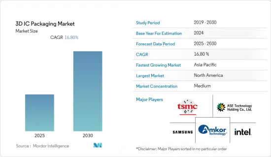
3D ICパッケージング市場は予測期間中にCAGR 16.8%を記録する見込み
主要ハイライト
- 成長するマイクロエレクトロニクスと半導体産業では、垂直積層集積回路(IC)の動向が発展しており、電子デバイスの要件を満たすために高性能、高機能、低消費電力を提供する実行可能なソリューションとして浮上しています。コネクテッドデバイス、タブレット、スマートフォンなどの電子製品では、エネルギー効率と性能を向上させ、テキストや通話以上のことを行うための先進的アーキテクチャに対するニーズが急増しています。このような要因が3D ICパッケージング市場の成長を後押しすると予想されます。
- 半導体用途の増加の結果、CMOSスケーリングの鈍化とコストの高騰により、産業はICのパッケージング先進に頼らざるを得なくなっています。3D積層技術は、機械学習、AI、データセンターなどの用途の要求性能を満たす有利なソリューションとして浮上しています。したがって、高性能コンピューティング用途に対するニーズの高まりが、予測期間にわたって3D-TSV(Through Silicon Via)市場を牽引しています。
- また、電子機器の小型化が進んでいることも市場成長の原動力になると予想されます。タブレット、スマートフォン、ゲーム機器における先進アーキテクチャへの需要の高まりと、センサやMEMSにおける先進ウエハーレベルパッケージング技術の利用の急増は、予測期間中、3D ICパッケージング市場に成長展望をもたらすと予想されます。WSTSによると、半導体のIC市場は2021年に4,630億米ドルの収益に達し、2022年には10%以上成長して5,109億6,000万米ドルになると予測されています。
- COVID-19パンデミックは様々な産業に大きな影響を与え、同時に世界中の先進医療機器とデバイスの開発を推進しました。さまざまな医療機器製造企業が、パンデミック発生後にいくつかの新しい機器やデバイスの生産を増やすことを発表しました。3D ICパッケージングの用途は医療産業で多数あるため、製造イニシアチブの増加は3D ICパッケージングの需要を押し上げると予想されます。
- しかし、初期投資の高さと半導体IC設計の複雑化が市場の進化を抑制すると予想されます。
3D ICパッケージング市場動向
IT・通信が大きな成長を遂げる見込み
- 3D ICパッケージングは、半導体の製造と設計に不可欠な要素です。マクロレベルでは性能、電力、コストに、ミクロレベルではすべてのチップの基本機能に直接影響します。
- 5Gインフラへの投資の増加や、IoT接続やネットワーキングデバイスと相まってデータセンター・サーバーの数が増加していることが、IT・通信セグメントにおける3D ICパッケージングの成長を後押しする要因となっています。例えば、韓国のKT、LG Uplus、SK Telecomなどの携帯電話事業者は、国全体で5Gインフラをサポートするために2022年までに総額25兆7,000億ウォンを投資することに合意しました。この追加投資は、ソウルをはじめとする6都市での5G品質強化に重点が置かれています。
- データセンターの拡大は、3D ICパッケージングを研究するベンダーに成長機会を記載しています。Cisco Systems Inc.によると、世界のデータセンター・ストレージのビッグデータ量は2021年に403エクサバイトに達すると予測されており、米国でのシェアが大きいです。ハイパースケールデータセンターは2015年の259から2021年には700に達します。
- さらに、IoT市場の開拓と、フットプリントの縮小と効率の向上が重要な無線技術に対する需要の急増により、3D ICパッケージング市場の発展が見込まれています。Ericsonによると、広域IoTデバイスは2021年の21億台から2027年には52億台に達します。
アジア太平洋は著しい成長率が見込まれる
- アジア太平洋には、TSMC、SMIC、UMC、韓国のSamsungといった大手半導体チップメーカーや企業があります。台湾の大手チップ鋳造会社は、重要な3ナノメートルチップ市場をリードする競争で日本のサプライヤーと提携しています。例えば、2021年2月、TSMCは日本の科学都市つくばに研究開発センターを設立し、日本のサプライヤーと協力して3D ICパッケージング材料を開発する予定であると発表しました。
- また、2021年5月、日本の経済産業省とその子会社である産業技術総合ラボは、約20社の日本企業がTSMCジャパンの3D IC研究開発センターと協力すると発表しました。
- アジア太平洋も3D ICパッケージング市場で大きなシェアを占めているが、これは同地域で相当数の半導体製造事業が行われていることに加え、Samsung Electronics、Toshiba Corporation、ASE Group、United Microelectronics Corp.などの大手市場参入企業が存在するためです。
- アジア太平洋は、自動車製造能力が高いことで知られています。さらに、自動車産業における5G技術の商業化の進展は、調査対象市場で事業を展開するベンダーに新たな収益源を記載しています。5G NRベースのC-V2Xの登場は、自律走行車に独自の機能を提供すると予想されます。そのため、より高いレベルの自律性と予測可能性、車両内の他のADASセンサ技術へのニーズが高まる可能性があります。
- さらに、この地域の市場参入企業は次世代チップ技術に力を入れており、3Dパッケージングツールによって新たな可能性を引き出す可能性があります。例えば、日本の工具メーカーであるディスコは、透明に近い薄さのシリコンウエハー上に集積回路を積層する3Dチップパッケージングに注力しています。ムーアの法則が物理的な限界に近づくなか、チップメーカーは次世代ハードウェアの性能を向上させるため、新たな設計や材料を模索しています。このような動向は、この地域の成長を促進すると予想されます。
- スマートデバイスとコネクテッドワールドの現在のシナリオでは、顧客はよりコンパクトで多機能、より優れた性能を提供し、消費電力が少ない次世代デバイスを求めています。このため、コスト効率が高く高性能なICへの需要が高まっています。例えば、STARのマイクロエレクトロニクスラボは、主要半導体企業と提携し、費用対効果の高い3Dウエハーレベル集積回路パッケージングソリューションを開発しています。同社は、大量生産向けのチップパッケージングソリューションを推進するため、チップオンウエハーコンソーシアムIIとコスト効率の高いインターポーザーコンソーシアムを立ち上げました。この産業に特化したコンソーシアムでは、ウエハーレベルパッケージングにおける主要課題に取り組み、製造コスト全体を低減することで、次世代電子機器の市場投入までの時間を短縮します。
3D ICパッケージング産業概要
世界の3D ICパッケージング市場は、 Amkor Technology Inc.、ASE Group、Siliconware Precision Industries(SPIL)などの大手企業の存在によりセグメント化されています。市場の参入企業は、常に先進的で包括的な製品を革新し続けなければならないです。
- 2021年5月:Intelは35億米ドルを投資してリオランチョ工場をアップグレードし、米国3大製造拠点の1つであるこの広大な複合施設の従業員数を35%以上増やす計画です。Intelは、フォベロス3Dパッケージング技術による新世代のチップを製造するため、ニューメキシコ工場を拡大します。
その他の特典
- エクセル形式の市場予測(ME)シート
- 3ヶ月間のアナリストサポート
目次
第1章 イントロダクション
- 調査の前提条件と市場定義
- 調査範囲
第2章 調査手法
第3章 エグゼクティブサマリー
第4章 市場洞察
- 市場概要
- 産業の魅力-ポーターのファイブフォース分析
- 新規参入業者の脅威
- 買い手/消費者の交渉力
- 供給企業の交渉力
- 代替品の脅威
- 競争企業間の敵対関係の強さ
- バリューチェーン分析
- COVID-19の市場への影響評価
第5章 市場力学
- 市場促進要因
- 電子製品におけるアーキテクチャの高度化
- 電子機器の小型化
- 市場課題/懸念事項
- 高い初期投資と半導体IC設計の複雑化
第6章 市場セグメンテーション
- パッケージング技術
- 3Dウエハーレベル・チップスケールパッケージング
- 3D TSV
- エンドユーザー産業
- 民生用電子機器
- 航空宇宙・防衛
- 医療機器
- 通信・電気通信
- 自動車
- その他
- 地域
- 北米
- 欧州
- アジア太平洋
- ラテンアメリカ
- 中東・アフリカ
第7章 競合情勢
- 企業プロファイル
- Taiwan Semiconductor Manufacturing Company Limited
- Samsung Electronics Co., Ltd.
- ASE Group
- Amkor Technology
- Intel Corporation
- Siliconware Precision Industries Co. Ltd(SPIL)
- GlobalFoundries
- Invensas
- Powertech Technology Inc.
第8章 投資分析
第9章 市場の将来
目次
Product Code: 91074
The 3D IC Packaging Market is expected to register a CAGR of 16.8% during the forecast period.
Key Highlights
- The growing microelectronics and semiconductor industry is developing a trend for vertically stacked integrated circuits (ICs), emerging as a viable solution for providing high performance, increased functionality, and reducing power consumption to fulfill electronic device requirements. The surging need for advanced architecture in electronic products such as connected devices, tablets, and smartphones to increase their energy efficiency and performance to do more than just texting and calling. Such factors are expected to bolster the growth of the 3D IC packaging market.
- As a result of the growing semiconductor applications, the slowdown in CMOS scaling and escalating costs have forced the industry to depend on packaging advancements for ICs. 3D stacking technologies have emerged as lucrative solutions that meet the required performance of applications such as machine learning, AI, and data centers. Therefore, the growing need for high-performance computing applications drives the 3D-TSV (Through Silicon Via) market over the forecast period.
- The increasing miniaturization of electronics devices is also anticipated to drive market growth. Growing demand for advanced architecture in tablets, smartphones, and gaming devices, along with surging usage of advanced wafer-level packaging technologies in sensors and MEMS, is expected to provide growth prospects for the 3D IC packaging market during the forecast period. According to WSTS, the IC market for semiconductors reached USD 463 billion in revenue in 2021 and is expected to grow by over 10% to USD 510.96 billion in 2022.
- The COVID-19 pandemic has significantly impacted various industries and has simultaneously propelled the development of advanced medical equipment and devices across the globe. Various medical equipment manufacturing companies announced to increase in the production of several new equipment and devices post the pandemic outbreak. As the applications of 3D IC packaging are numerous within the medical and healthcare industry, the increased manufacturing initiatives are expected to boost the demand for 3D IC packaging.
- However, the high Initial Investment and Increasing Complexity of Semiconductor IC Designs are expected to restrain the evolution of the market.
3D IC Packaging Market Trends
IT & Telecommunication is Expected to Witness Significant Growth
- 3D IC Packaging is an essential part of semiconductor manufacturing and design. It directly affects performance, power, and cost on a macro level and the basic functionality of all chips on a micro level.
- The increasing investment in 5G infrastructure and the growing number of data center servers coupled with IoT connections and networking devices are the factors propelling the growth of 3D IC packaging in the IT and telecommunication sector. For instance, mobile operators in Korea such as KT, LG Uplus, and SK Telecom agreed to invest a total of KRW 25.7 trillion through 2022 to support 5G infrastructure across the country. The additional investment is focused on enhancing the 5G quality in Seoul and six other cities.
- The expansion of data centers provides a growth opportunity for the vendors in the 3D IC packaging studied. According to Cisco Systems, the amount of big data in data center storage global is anticipated to reach 403 exabytes in 2021, with a significant share in the US. Hyperscale data centers reached 700 in 2021, compared to 259 in 2015.
- Moreover, the growing IoT market and surging demand for wireless technologies, wherein reduced footprint and enhanced efficiency are critical, are expected to develop the market for 3D IC packaging. According to Ericson, wide-area IoT devices will reach 5.2 billion by 2027 from 2.1 billion in 2021.
Asia-Pacific is Expected to Witness Significant Growth Rate
- Asia Pacific is home to some of the biggest semiconductor chip manufacturers and companies like TSMC, SMIC, UMC, and South Korea's Samsung. Taiwan's leading chip foundry is teaming up with Japanese suppliers in the race to lead the crucial 3-nanometer chip market. For instance, in February 2021, TSMC announced that the company plans to establish an R&D center in Japan's science city of Tsukuba to develop 3D IC packaging materials in cooperation with its Japanese suppliers.
- Also, in May 2021, Japan's Ministry of Economy, Trade, and Industry and its subsidiary, the National Institute of Advanced Industrial Science and Technology, announced that approximately 20 Japanese companies would work with TSMC Japan's 3D IC R&D Center.
- The Asia Pacific region also holds a significant share in the 3D IC packaging market due to a considerable number of semiconductor manufacturing operations happening in the region, along with the presence of major market players such as Samsung Electronics Co., Ltd., Toshiba Corp, ASE Group, and United Microelectronics Corp. among others.
- The Asia Pacific region is known for its robust Automotive manufacturing capabilities. Moreover, the growing commercialization of 5G technology in the automotive industry will provide a new revenue stream for the vendors operating in the studied market. The advent of 5G NR-based C-V2X is anticipated to offer unique capabilities for the autonomous vehicle. Thus, it can propel the need for higher levels of autonomy and predictability and other ADAS sensor technologies in the vehicle.
- Additionally, market players in the region are forcing on Next-gen chip technology, which could unlock new potential with 3D packaging tools. For instance, Japanese tool-making company Disco focuses on 3D chip packaging by stacking integrated circuits on silicon wafers of near-transparent thinness. As Moore's Law nears its physical limits, chipmakers seek new designs and materials to get better performance out of next-generation hardware. Such trends are expected to propel growth in the region.
- In the current scenario of smart devices and the connected world, customers demand next-generation devices that are more compact, multi-functional, offer better performance, and consume less power. This has propelled the demand for cost-efficient and high-performance IC. For instance, STAR's Institute of Microelectronics has partnered with leading semiconductor companies to develop cost-effective 3D wafer-level integrated circuit packaging solutions. The company has launched chip-on-wafer consortium II and the cost-effective Interposer consortium to advance chip packaging solutions for high-volume manufacturing. The industry-focused consortium will address key challenges in wafer-level packaging to low overall manufacturing costs to accelerate time-to-market for next-generation electronics devices.
3D IC Packaging Industry Overview
The Global 3D IC Packaging Market is fragmented due to the presence of significant players such as Amkor Technology Inc., ASE Group, and Siliconware Precision Industries Co. Ltd (SPIL), among others. The market players must constantly innovate advanced and comprehensive products to stay relevant.
- In May 2021: Intel plans to invest USD 3.5 billion to upgrade its Rio Rancho plant and increase its headcount by more than 35% at the sprawling complex, one of its three largest US manufacturing hubs. It is expanding its New Mexico operations to manufacture new generations of chips based on its Foveros 3D packaging technology, which could aid the company's attempts to regain its leadership status in the semiconductor industry.
Additional Benefits:
- The market estimate (ME) sheet in Excel format
- 3 months of analyst support
TABLE OF CONTENTS
1 INTRODUCTION
- 1.1 Study Assumptions and Market Definition
- 1.2 Scope of the Study
2 RESEARCH METHODOLOGY
3 EXECUTIVE SUMMARY
4 MARKET INSIGHT
- 4.1 Market Overview
- 4.2 Industry Attractiveness - Porter's Five Forces Analysis
- 4.2.1 Threat of New Entrants
- 4.2.2 Bargaining Power of Buyers/Consumers
- 4.2.3 Bargaining Power of Suppliers
- 4.2.4 Threat of Substitute Products
- 4.2.5 Intensity of Competitive Rivalry
- 4.3 Value Chain Analysis
- 4.4 Assessment of the Impact of COVID-19 on the Market
5 MARKET DYNAMICS
- 5.1 Market Drivers
- 5.1.1 Growing Advanced Architecture in Electronic Products
- 5.1.2 Miniaturization of Electronics Devices
- 5.2 Market Challenges/Restrains
- 5.2.1 High Initial Investment and Increasing Complexity of Semiconductor IC Designs
6 MARKET SEGMENTATION
- 6.1 Packaging Technology
- 6.1.1 3D wafer-level chip-scale packaging
- 6.1.2 3D TSV
- 6.2 End-User Industry
- 6.2.1 Consumer electronics
- 6.2.2 Aerospace and Defense
- 6.2.3 Medical Devices
- 6.2.4 Communications and Telecom
- 6.2.5 Automotive
- 6.2.6 Others
- 6.3 Geography
- 6.3.1 North America
- 6.3.2 Europe
- 6.3.3 Asia-Pacific
- 6.3.4 Latin America
- 6.3.5 Middle-East and Africa
7 COMPETITIVE LANDSCAPE
- 7.1 Company Profiles
- 7.1.1 Taiwan Semiconductor Manufacturing Company Limited
- 7.1.2 Samsung Electronics Co., Ltd.
- 7.1.3 ASE Group
- 7.1.4 Amkor Technology
- 7.1.5 Intel Corporation
- 7.1.6 Siliconware Precision Industries Co. Ltd (SPIL)
- 7.1.7 GlobalFoundries
- 7.1.8 Invensas
- 7.1.9 Powertech Technology Inc.
8 INVESTMENT ANALYSIS
9 FUTURE OF THE MARKET
3D ICパッケージング:市場シェア分析、産業動向と統計、成長予測(2025~2030年)
- 発行日
- 発行
- Mordor Intelligence
- ページ情報
- 英文 120 Pages
- 納期
- 2~3営業日