
|
市場調査レポート
商品コード
1940700
ダイシング装置:市場シェア分析、業界動向と統計、成長予測(2026年~2031年)Dicing Equipment - Market Share Analysis, Industry Trends & Statistics, Growth Forecasts (2026 - 2031) |
||||||
カスタマイズ可能
適宜更新あり
|
|||||||
| ダイシング装置:市場シェア分析、業界動向と統計、成長予測(2026年~2031年) |
|
出版日: 2026年02月09日
発行: Mordor Intelligence
ページ情報: 英文 137 Pages
納期: 2~3営業日
|

概要
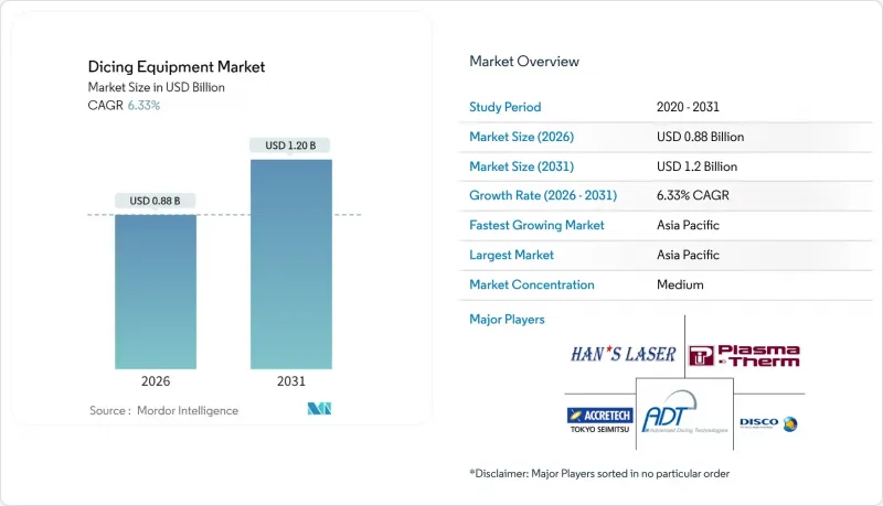
ダイシング装置市場の規模は、2026年には8億8,000万米ドルと推定されており、2025年の8億3,000万米ドルから成長が見込まれます。
2031年の予測では12億米ドルに達し、2026年から2031年にかけてCAGR6.33%で拡大する見通しです。
半導体バックエンド製造分野、特に薄型ウェーハ、先進パッケージング技術、ワイドバンドギャップパワーデバイスへの堅調な投資が、この着実な拡大を支えています。電気自動車、再生可能エネルギー、AIワークロードの需要が高まる中、チップメーカーは高歩留まりのダイ分離を優先し、サブマイクロメートル単位の位置決め精度、汚染管理された加工プロセス、統合検査機能を兼ね備えたシステムを重視しています。3Dおよびヘテロジニアス集積への継続的な移行により、欠けを最小限に抑え、より狭いストリートを実現するプラズマおよびレーザーダイシング装置の需要が高まっています。一方、自動化の高度化は、ファブが労働力不足を補い、工程切り替え時間を短縮し、総合設備効率(OEE)を向上させるのに貢献しています。米国、欧州、東アジアにおけるサプライチェーンの地域化プログラムは新たな地域需要拠点をもたらしていますが、希土類レーザー光源をめぐる持続的な地政学的摩擦や、スラリー廃棄に関する厳格な規制により、資本集約度は依然として高い水準を維持しています。
世界のダイシング装置市場の動向と洞察
高精度モーションシステムの技術的進歩
最近のモーション制御技術の革新により、ヘテロジニアス統合ラインに不可欠なサブマイクロメートル単位のステージ精度が実現されました。例えば、DISCO社のDFD6370プラットフォームは、330×330mm基板を処理しながら、切断深さを±1μm以内に維持する選択可能な高さセンサーを採用しており、パネルレベルパッケージングにおいて優位性を発揮します。アクティブダンピング、閉ループロボット技術、ビジョンガイドによる位置合わせにより、振動や熱ドリフトをさらに低減し、脆い炭化ケイ素ウエハーの加工時に高い歩留まりを実現します。オンボード計測機能を備えた多軸ステージを統合するベンダーは、切断、洗浄、検査を単一フローで組み合わせたターンキー方式のシングレーションセルを提供し、ハンドリング欠陥とサイクルタイムを削減しています。
先進ロジック・メモリ工場からの需要急増
SEMIの予測によれば、2025年から2027年にかけての300mmファブ向け設備投資総額は4,000億米ドルに達し、そのうち鋳造が2,300億米ドルを占める見込みです。新たな極端紫外線(EUV)プロセスノードおよび3D積層DRAMラインの導入により、裏面汚染リスクが増大しており、ファブでは静電気抑制機能と密閉型チップ回収機能を備えたダイシング装置の採用が求められています。特にTSMC、サムスン、中国国内のファウンドリにおいて生産能力の拡大が加速する中、装置サプライヤーにとって、迅速な装置納入とフィールドサービス網の拡充が調達における重要な判断基準となっています。
スラリー・化学薬品廃棄規制の強化
ISO 14644クリーンルーム規格の改訂および新たなPFAS規制により、ファブでは廃水ループの改修、フッ素化合物除去システムの設置、クローズドループ冷却剤の採用が求められています。ダイシングセル内にリサイクルモジュールとリアルタイム粒子モニターを組み込んだベンダーは、顧客が規制基準を満たしつつ光熱費を削減する支援を行っています。ただし、追加設備コストと施設改修により、購入決定が遅れるケースも見られます。
セグメント分析
2025年時点でダイシング装置市場の46.10%をブレードシステムが占めております。ウェハー当たりのコスト優位性と成熟したサービスネットワークが、大量生産のロジック・メモリラインに適しているからです。しかしながら、50µm未満のウェハーが普及する中、レーザーセグメントは6.53%のCAGRで拡大しております。これは従来のブレードでは保証できない、切れ目なしのシングレーション(個片化)が求められるためです。パナソニックのAPX300プラズマプラットフォームは300mmウェーハ上で20µmのストリート幅を実現し、プラズマ・レーザー工具がもたらす性能飛躍を裏付けています。ブレードによる粗切断とレーザー仕上げを組み合わせたハイブリッドラインも普及が進み、スループットとダイ強度のバランスを実現しています。
レーザー光学系、希土類アライメント部品、数kW級電源装置の追加コストは、価格に敏感なファブでの導入を依然として制限しています。しかしながら、ダイ・トゥ・パッケージの垂直配線や脆性SiC基板が主流となる分野では、初期投資の高さは、廃棄率の低減と設計ルールの厳格化によって相殺されます。予測期間においては、超高速パルス整形技術とオートフォーカス光学系の持続的な研究開発により、装置の稼働率が向上し、ウェーハ単価のコスト差が徐々に縮小することが見込まれます。
半導体業界ではより大型のウェーハフォーマットへの移行が進んでおり、450mmを超えるウェーハは2031年までCAGR6.38%で成長し、2025年に37.55%の市場シェアを占めた300mmウェーハに迫ると予測されます。先進的なパッケージング用途、特にパネルレベルパッケージング工程では、より大型の基板処理能力への需要が高まっています。ディスコ株式会社のDFD6370は最大330×330mmのワークピースに対応し、従来のウェーハ処理と新興の大判要求とのギャップを埋めるものです。
200mm以下の小型ウェーハは、MEMSデバイスやパワー半導体など特殊用途において依然として重要性を保っています。基板コストやプロセス最適化の観点から、確立されたフォーマットが有利となる分野です。200mmセグメントは成熟ノードの拡大と自動車用半導体需要の恩恵を受けており、150mmウェーハは化合物半導体やレガシーデバイス生産のニッチ用途で活用されています。しかしながら、基板あたりのダイ歩留まり向上や単位処理コスト削減など、大型ウェーハの経済的優位性がフォーマット移行を推進しております。SEMIの「World Fab Forecast」では、2027年までに操業開始が見込まれる高確率の製造施設79ヶ所を特定しており、その多くが混合ウェーハサイズ対応能力を備えております。単一プラットフォーム内で複数ウェーハフォーマットに対応する拡張性のあるハンドリングシステムを開発する装置メーカーは、この進化する環境において優位な立場にあります。
地域別分析
アジア太平洋地域は、台湾、韓国、日本、中国本土に根付いた製造クラスターに支えられ、2025年においてもダイシング装置市場の42.55%のシェアを維持しました。東京政府による総額3兆9,000億円(260億米ドル)の補助金支援が日本の復活を支え、精密モーションベンダーや自動化インテグレーターへの受注を促進しています。中国のOSAT(受託組立サービス)企業は、自社設計のAIアクセラレータの歩留まり向上に向け、プラズマダイシングラインの導入を加速させています。一方、東南アジア諸国では組立業務の波及効果により、中規模ブレードダイサーの需要が生まれています。
北米のCHIPS法は500億米ドル超の優遇措置を可能とし、アリゾナ州、テキサス州、ニューヨーク州北部の新規工場を2026年以降の新たな調達拠点へと変貌させています。これらの拠点では、熟練労働者不足を補うため、予知保全分析機能を備えた完全自動化ブレード/レーザーセルの導入を優先しています。
欧州のチップス法は470億米ドルを大陸の生産能力に投入し、ドイツとフランスのプロジェクトがEVサプライチェーン向け炭化ケイ素パワーエレクトロニクスを主導しています。アジアの生産量には及ばないもの、EUファブにおける厳格な環境基準が閉ループスラリーや低水消費プラズマダイシングシステムの導入を加速させ、地域の平均販売価格(ASP)を押し上げています。
その他の特典:
- エクセル形式の市場予測(ME)シート
- アナリストによる3ヶ月間のサポート
よくあるご質問
目次
第1章 イントロダクション
- 調査の前提条件と市場の定義
- 調査範囲
第2章 調査手法
第3章 エグゼクティブサマリー
第4章 市場情勢
- 市場概要
- 市場促進要因
- 高精度モーションシステムにおける技術的進歩
- 先進ロジックおよびメモリ製造工場からの需要急増
- 3Dパッケージングおよびヘテロジニアス集積の急速な普及
- 電気自動車(EV)および再生可能エネルギー向けパワーデバイスの導入拡大
- 超薄型ウェーハ向けプラズマダイシングへの移行
- 中国における国産設備の現地化インセンティブ
- 市場抑制要因
- 高額な設備投資と長い回収期間
- 欠けや微細なひび割れによる歩留まり損失
- スラリー・化学薬品廃棄に関する規制の強化
- レーザー光源の供給ボトルネックと希土類依存性
- マクロ経済要因が市場に与える影響
- 業界サプライチェーン分析
- 規制情勢
- テクノロジーの展望
- ポーターのファイブフォース分析
- 新規参入業者の脅威
- 買い手・消費者の交渉力
- 供給企業の交渉力
- 代替品の脅威
- 競争企業間の敵対関係
第5章 市場規模と成長予測
- 技術分野別
- ブレードダイシング
- レーザーアブレーション
- ステルスダイシング
- プラズマダイシング
- ウエハーサイズ別
- 150 mm以下
- 200 mm
- 300 mm
- 450 mm以上
- 用途別
- ロジックとメモリ
- MEMSデバイス
- パワーデバイス
- CMOSイメージセンサー
- RFID/スマートカード
- エンドユーザー業界別
- ファウンドリ
- IDM
- OSAT
- 地域別
- 北米
- 米国
- カナダ
- メキシコ
- 南米
- ブラジル
- アルゼンチン
- その他南米
- 欧州
- ドイツ
- 英国
- フランス
- イタリア
- スペイン
- ロシア
- その他欧州地域
- アジア太平洋地域
- 中国
- 日本
- インド
- 韓国
- 東南アジア
- その他アジア太平洋地域
- 中東・アフリカ
- 中東
- サウジアラビア
- アラブ首長国連邦
- その他中東
- アフリカ
- 南アフリカ
- エジプト
- その他アフリカ
- 中東
- 北米
第6章 競合情勢
- 市場集中度
- 戦略的動向
- 市場シェア分析
- 企業プロファイル
- DISCO Corporation
- Tokyo Seimitsu Co., Ltd.(ACCRETECH)
- Advanced Dicing Technologies Ltd.
- Panasonic Connect Co., Ltd.
- SPTS Technologies Ltd.(KLA Corporation)
- Plasma-Therm LLC
- Veeco Instruments Inc.
- Synova SA
- 3D-Micromac AG
- Han's Laser Technology Industry Group Co., Ltd.
- Suzhou Delphi Laser Co., Ltd.
- EO Technics Co., Ltd.
- Neon Tech Co., Ltd.
- ASM Laser Separation International B.V.
- Kulicke & Soffa Industries, Inc.
- Takatori Corporation
- Lumentum Holdings Inc.(dicing lasers)
- IPG Photonics Corporation
- Oxford Instruments Plasma Technology
- Plasma Etch Inc.
- Dynatex International
- Loadpoint Micro Machining Ltd.
- Disco Hi-Tec America, Inc.
- Shenzhen JLH Laser Co., Ltd.
- Wuhan HGLaser Engineering Co., Ltd.
