
|
市場調査レポート
商品コード
1687872
パネルレベル包装:市場シェア分析、産業動向と統計、成長予測(2025~2030年)Panel Level Packaging - Market Share Analysis, Industry Trends & Statistics, Growth Forecasts (2025 - 2030) |
||||||
カスタマイズ可能
適宜更新あり
|
|||||||
| パネルレベル包装:市場シェア分析、産業動向と統計、成長予測(2025~2030年) |
|
出版日: 2025年03月18日
発行: Mordor Intelligence
ページ情報: 英文 112 Pages
納期: 2~3営業日
|

全表示
- 概要
- 目次
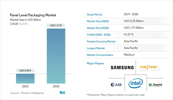
パネルレベル包装市場規模は2025年に3億5,000万米ドルと推定され、予測期間(2025~2030年)のCAGRは41.07%で、2030年には19億7,000万米ドルに達すると予測されます。
半導体産業は急速な成長を遂げており、半導体はあらゆる現代技術の基本コンポーネントとなっています。このセグメントの進歩や革新は、下流のすべての技術に直接影響を与え、市場調査の必要性を後押ししています。
主要ハイライト
- 半導体産業の重要性が高まるにつれ、包装ソリューションの強化に対する需要も高まり、新しい半導体包装技術の開発につながっています。
- パネルレベル包装(PLP)は、最近脚光を浴びている技術です。PLPは、パネルサイズで処理される半導体包装を指します。パネルレベル包装では、組立プロセスに、パネルレベルでのダイアタッチ、再配線、モールド、バンプの製造が含まれます。
- パネル・パラレル・フォーマットでは、より多くの包装が処理されるため、このタイプの包装では、ラウンド・ウエハー形態と比較して、はるかに優れた面積利用(パネル/ウエハー・サイズと包装・サイズの比率)が容易になります。したがって、包装コストの低減が市場成長の主要促進要因の一つとなっています。PLPは廃棄物の発生やカーボンフットプリントが少ないため、環境への影響も少ないです。
- パネルレベル包装(PLP)市場には課題もあります。この技術に関連する多額の費用と、その実装の複雑な性質が、広く受け入れられる妨げになる可能性があります。包装プロセスには、金型先行型とRDL先行型があります。しかし、包装のタイプによってダイシフトに問題が生じます。ダイシフトは、歩留まりの低下や歩留まりに悪影響を及ぼす可能性があるため、最大の問題の一つと考えられています。このため、包装プロセスをより詳細に管理する必要性が高まり、複雑さが増して市場の成長を抑制しています。
- COVID-19以降では、コスト面でのメリットや、ウエハーから大型パネルフォーマットへの包装サイズの拡大により、パネルレベル包装への注目が高まると予想されます。並行して製造される包装の数が増えることも、市場の成長を支える大きな利点です。PLPは、他の技術セグメントのプロセス、材料、設備を採用する可能性があります。プリント回路基板(PCB)、液晶ディスプレイ(LCD)、ソーラー機器などはパネルサイズで製造されており、ファンアウト型のパネルレベル包装に新たなアプローチを提供しています。
パネルレベル包装市場動向
市場セグメンテーションはコンシューマーエレクトロニクスセグメントが主要シェアを占める
- スマートフォン、ウェアラブル端末、タブレット端末などの民生用電子機器製品は、薄型化・小型化が進んでいます。小型化・軽量化のニーズに対応するため、PLPによってメーカーは部品密度を高め、スペースをより効率的に利用することができます。これらの機器にとって、PLPによるフットプリントの縮小は、洗練されたデザインを可能にし、利用可能なスペースを最大限に活用するために不可欠です。
- 民生用電子機器産業は、製品の差別化に努めるメーカーと競合しています。民生用電子機器の洗練されたデザイン、機能性の向上、性能の改善を可能にすることで、PLPは市場に優位性をもたらします。市場での地位を維持するため、メーカーはPLPを活用して消費者の需要を満たし、革新的な製品を投入しています。
- 近年、5GとIoTの普及が進んでいることは、市場に大きな成長機会をもたらしています。例えば、5G Americasによると、世界の5G加入件数は2024年に28億件、2027年には59億件に達すると推定されています。
- 5Gへの投資の高まりに伴い、5G対応スマートフォンの需要も並行して増加しています。サイバーメディアリサーチのレポートによると、2020年の初導入以来、5Gスマートフォンの販売台数が13倍を記録した後、2023年末までに5Gスマートフォンの出荷台数は毎年70%増加しました。2020年にはわずか4%だった5Gスマートフォンの市場シェアは、2023年には45%に達すると予測されています。
- 同様に、インターネットとIP対応プロトコルを使用してモノと人との通信を可能にする技術であるモノのインターネット(IoT)の採用が増加しているため、接続されたデバイスの数は近年急速に増加しています。例えば、シスコによれば、2023年にはネットワーク接続されたデバイスの数は293億台になるといいます。IoTユースケースの大幅な拡大は、市場成長の大きな原動力となると考えられます。
中国が市場をリードする見込み
- 中国は最大の半導体消費国であり、その主要理由は国内電子機器市場の規模にあります。同国は世界最大の民生用電子機器の生産・輸出国であり、安価な労働コストのメリットを活用するため、多くの世界ベンダーが施設を設立しています。
- 電子機器製造業も最近、着実な拡大を続けています。工業・情報化部の報告書によると、2023年、電子情報製造部門の主要企業の産業付加価値は年率3.4%増となりました。同省によると、主要製品のうち、携帯電話の生産台数は前年比6.9%増の15億7,000万台で、このうちスマートフォンの台数は前年比1.9%増の11億4,000万台でした。近年、エレクトロニクス産業の成長を後押しするため、いくつかの取り組みが行われています。
- また、中国は5Gの普及でも世界をリードしています。工業情報化省(MIIT)によると、中国は2023年2月時点で5億9,201万人の5Gユーザーを目指しています。この数は2025年までに10億人を突破すると予想されています。中国全土に5Gの普及を拡大するため、インフラ整備が進められています。
- 例えば、2023年10月現在、中国の5G基地局は約322万局で、モバイル基地局全体の28.1%を占めています。
- 国内での5Gの導入が進むにつれ、5G対応デバイスの普及も進んでいます。例えば、中国情報通信技術研究院(CAICT)によると、2023年の同国における5Gスマートフォンの出荷台数は前年比約11.9%増の2億4,000万台に達し、スマートフォン出荷市場全体は前年比約1.1%増となりました。先進包装技術は5Gチップの性能要件の多くを解決するのに役立つ可能性があるため、こうした動向は同国における研究市場の成長に有利に働くと予想されます。
- また、中国は生産と消費の両面で自動車市場をリードしており、同国の市場成長にも有利に働くと予想されます。よりクリーンで安全な自動車に対する需要の高まりは、同国の自動車産業における主要動向のひとつであり、調査対象市場の成長を後押ししています。自律走行車、電動化、キャビンの充実、接続性とソフトウェア定義、ゾーンアーキテクチャなどの市場メガ動向も、自動車セグメントの市場成長を支えています。
パネルレベル包装産業概要
パネルレベル包装市場は、Samsung Electronics、Intel Corporation、Nepes Corporation、ASE Group、Powertech Technology Inc.などの大手企業が存在し、半固体化しています。市場の参入企業は、製品ラインナップを強化し、サステイナブル競争優位性を獲得するために、提携や買収などの戦略を採用しています。
- 2023年12月-NEPESがエッジコンピューティング用インテリジェント半導体「METIS」を開発。Metisは、ネペスの最先端2.5D&3D包装プラットフォームであるnePACTMのcx-BGA(Ball Grid Array)を採用しました。nePACTMは、ファンアウト技術とフリップチップボンディング技術をベースに、多層・微細RDL配線を実現した次世代の最先端包装技術です。人工知能半導体などの高集積・高性能チップに適しています。
- 2023年6月-ASE Technology Holdingの子会社であるUSIがポーランドに工場を設立。この動きは、欧州顧客からの同社製品に対するニーズの高まりを反映したものです。拡大により、USIはポーランドでより多くの製品を製造し、顧客のニーズに応え、市場の成長に対応することができます。
その他の特典
- エクセル形式の市場予測(ME)シート
- 3ヶ月間のアナリストサポート
目次
第1章 イントロダクション
- 調査の前提条件と市場定義
- 調査範囲
第2章 調査手法
第3章 エグゼクティブサマリー
第4章 市場洞察
- 市場概要
- 産業の魅力-ポーターのファイブフォース分析
- 供給企業の交渉力
- 買い手の交渉力
- 新規参入業者の脅威
- 代替品の脅威
- 競争企業間の敵対関係の強さ
- 産業バリューチェーン/サプライチェーン分析
- マクロ経済要因が市場に与える影響の評価
第5章 市場力学
- 市場促進要因
- 包装プロセスのコスト削減
- 小型で高機能な電子機器への需要の高まり
- 研究開発投資の増加
- 市場抑制要因
- 包装プロセスの複雑化
第6章 市場セグメンテーション
- 産業別用途
- コンシューマーエレクトロニクス
- 自動車
- 通信
- その他の産業用途
- 地域別
- 米国
- 中国
- 韓国
- 台湾
- 日本
- 欧州
- その他
第7章 競合情勢
- 企業プロファイル
- Samsung Electronics Co. Ltd
- Intel Corporation
- Nepes Corporation
- ASE Group
- Powertech Technology Inc.
- Fraunhofer Institute for Reliability and Micro integration IZM
- Unimicron Technology Corporation
- DECA Technologies Inc.
- JCET/STATSChipPAC
第8章 投資分析
第9章 市場の将来
The Panel Level Packaging Market size is estimated at USD 0.35 billion in 2025, and is expected to reach USD 1.97 billion by 2030, at a CAGR of 41.07% during the forecast period (2025-2030).
The semiconductor industry is witnessing rapid growth, with semiconductors emerging as the basic building blocks of all modern technology. The advancements and innovations in this field directly impact all downstream technologies and drive the need for the market studied.
Key Highlights
- With the importance of the semiconductor industry growing, the demand for enhanced packaging solutions is also increasing, leading to the development of new semiconductor packaging techniques.
- Panel-level packaging (PLP) is a technology that has gained prominence recently. PLP refers to semiconductor packaging processed on a panel size. In panel-level packaging, the assembly process includes the fabrication of die attach, redistribution lines, molding, and bumping at the panel level.
- As more packages may be processed in panel and parallel formats, this type of packaging facilitates a much better area utilization (ratio between panel/wafer size and package size) compared to round wafer shapes. Hence, a lower packaging cost is among the primary drivers for the market's growth. PLP has a lower environmental impact due to a lower waste generation and carbon footprint.
- The panel-level packaging (PLP) market also encounters certain challenges. The substantial expenses linked to the technology and the intricate nature of its implementation might impede its extensive acceptance. The packaging process involves both types, mold first and RDL first. However, the type of packaging involves problems in die shift. Shifting the die is considered one of the biggest issues as it may cause lesser yield or negatively influence the yields. This increases the need for more control over the packaging process and adds complexity, restraining the market's growth.
- In the post-COVID-19 period, the focus on panel-level packaging is anticipated to increase due to the cost benefits and the expansion of the packaging size from wafers to larger panel formats. Increasing the number of packages manufactured in parallel is another major advantage supporting the market's growth. PLP may adopt processes, materials, and equipment from other technology areas. Printed circuit boards (PCB), liquid crystal displays (LCD), or solar equipment are manufactured on panel sizes and offer new approaches for fan-out panel-level packaging.
Panel Level Packaging Market Trends
Consumer Electronics Segment to Hold Major Market Share
- Consumer electronics such as smartphones, wearables, and tablets are becoming increasingly thin and compact. To meet the needs of miniaturization and light form factors, PLP allows manufacturers to achieve greater component density and more efficient use of space. For these devices, the reduced footprint caused by PLP is essential as it will enable sleek designs and maximize their utilization of available space.
- The consumer electronics industry competes with manufacturers who strive to differentiate products. By enabling sleek designs, increased functionality, and improved performance for consumer electronics devices, PLP provides an advantage to the market. To maintain their position in the market, manufacturers take advantage of PLP to meet consumer demands and introduce innovative products.
- The increasing penetration of 5G and IoT in recent years presents significant growth opportunities for the market. For instance, as per 5G Americas, the 5G subscriptions worldwide are estimated to reach 2.8 billion in 2024 and 5.9 billion by 2027.
- With the rising investments in 5G, the demand for 5G-enabled smartphones is also increasing parallelly. According to a report from Cybermedia Research, by the end of 2023, after recording a 13 times increase in 5G smartphone sales since its first introduction in 2020, shipments of 5G smartphones increased by 70% yearly. From only 4% in 2020, 5G smartphones were projected to capture a possible 45% market share in 2023.
- Similarly, owing to the rising adoption of the Internet of Things (IoT), the technology that enables communications between things and people using the Internet and IP-enabled protocols, the number of connected devices has been increasing rapidly in recent years. For instance, as per Cisco, there would be 29.3 billion networked devices in 2023. The massive expansion in IoT use cases will provide a significant impetus to market growth.
China is Expected to Lead the Market
- China is the largest semiconductor consumer, primarily due to the size of the domestic electronics market. The country is the world's largest producer and exporter of consumer electronics, as a significantly more significant number of global vendors have established their facilities to leverage the benefits of cheap labor costs.
- The electronics manufacturing industry has also recently continued to maintain steady expansion. As per a report by the Ministry of Industry and Information Technology via China Daily, in 2023, the industrial added value of major companies in the electronic information manufacturing sector grew by 3.4% yearly. According to the ministry, among significant products, the output of mobile phones increased by 6.9% Y-o-Y to 1.57 billion units, within which the number of smartphones increased by 1.9% Y-o-Y to 1.14 billion units. Several initiatives have been taken in recent years to boost the electronics industry's growth.
- China also leads in 5G adoption globally. According to the Ministry of Industry and Information Technology (MIIT), China aims to have 592.01 million 5G users as of February 2023. This number is anticipated to surpass 1 billion mark by 2025. A combined effort is being made to develop the supporting infrastructure to expand the footprint of 5G across the country.
- For instance, as of October 2023, China had about 3.22 million 5G base stations, constituting 28.1% of its entire mobile base station.
- The growing implementation of 5G in the country has also increased the uptake of 5G-enabled devices. For instance, according to the China Academy of Information and Communications Technology (CAICT), in 2023, 5G smartphone shipments in the country grew by about 11.9% Y-o-Y to 240 million units, while the overall smartphone shipments market grew by about 1.1%, compared to the previous year. As advanced packaging technologies may help resolve many of the 5G chip performance requirements, such trends are anticipated to favor the studied market's growth in the country.
- China is also a leading automotive market in production and consumption, which is anticipated to favor the market's growth in the country. The rising demand for cleaner and safer vehicles is among the major trends in the country's automotive industry, which supports the studied market's growth. Industry megatrends, including autonomous vehicles, electrification, enriched cabins, connectivity and software definition, and zonal architecture, also support the market's growth in the automotive segment.
Panel Level Packaging Industry Overview
The panel level packaging market is semi-consolidated with the presence of major players like Samsung Electronics Co. Ltd, Intel Corporation, Nepes Corporation, ASE Group, and Powertech Technology Inc. Players in the market are adopting strategies such as partnerships and acquisitions to enhance their product offerings and gain sustainable competitive advantage.
- December 2023 - NEPES developed 'METIS,' an intelligent semiconductor for edge computing. Metis applied cx-BGA (Ball Grid Array) of nePACTM, Nepes' cutting-edge 2.5D & 3D package platform. nePACTM is a next-generation cutting-edge package technology that implements multi-layer and fine RDL wiring based on fan-out technology and flip-chip bonding technology. It is suitable for highly integrated, high-performance chips such as artificial intelligence semiconductors.
- June 2023 - USI, a subsidiary of ASE Technology Holding Co. Ltd, inaugurated another factory in Poland. This move reflects the growing need for the company's products from European customers. By expanding, USI may make more goods in Poland, meet customer needs, and keep up with market growth.
Additional Benefits:
- The market estimate (ME) sheet in Excel format
- 3 months of analyst support
TABLE OF CONTENTS
1 INTRODUCTION
- 1.1 Study Assumptions and Market Definition
- 1.2 Scope of the Study
2 RESEARCH METHODOLOGY
3 EXECUTIVE SUMMARY
4 MARKET INSIGHTS
- 4.1 Market Overview
- 4.2 Industry Attractiveness - Porter's Five Forces Analysis
- 4.2.1 Bargaining Power of Suppliers
- 4.2.2 Bargaining Power of Buyers
- 4.2.3 Threat of New Entrants
- 4.2.4 Threat of Substitute Products
- 4.2.5 Intensity of Competitive Rivalry
- 4.3 Industry Value Chain/Supply Chain Analysis
- 4.4 Assessment of Impact of Macroeconomic Factors on the Market
5 MARKET DYNAMICS
- 5.1 Market Drivers
- 5.1.1 Reduced Cost of Packaging Process
- 5.1.2 Increasing Demand for Compact and High Functionality Electronic Devices
- 5.1.3 Increased Investment on Research and Development Activities
- 5.2 Market Restraints
- 5.2.1 Complexity in Packaging Process
6 MARKET SEGMENTATION
- 6.1 By Industry Application
- 6.1.1 Consumer Electronics
- 6.1.2 Automotive
- 6.1.3 Telecommunication
- 6.1.4 Other Industry Applications
- 6.2 By Geography
- 6.2.1 United States
- 6.2.2 China
- 6.2.3 Korea
- 6.2.4 Taiwan
- 6.2.5 Japan
- 6.2.6 Europe
- 6.2.7 Rest of the World
7 COMPETITIVE LANDSCAPE
- 7.1 Company Profiles
- 7.1.1 Samsung Electronics Co. Ltd
- 7.1.2 Intel Corporation
- 7.1.3 Nepes Corporation
- 7.1.4 ASE Group
- 7.1.5 Powertech Technology Inc.
- 7.1.6 Fraunhofer Institute for Reliability and Micro integration IZM
- 7.1.7 Unimicron Technology Corporation
- 7.1.8 DECA Technologies Inc.
- 7.1.9 JCET/ STATSChipPAC
