
|
市場調査レポート
商品コード
1687834
リン化インジウムウエハ-市場シェア分析、産業動向・統計、成長予測(2025年~2030年)Indium Phosphide Wafer - Market Share Analysis, Industry Trends & Statistics, Growth Forecasts (2025 - 2030) |
||||||
カスタマイズ可能
適宜更新あり
|
|||||||
| リン化インジウムウエハ-市場シェア分析、産業動向・統計、成長予測(2025年~2030年) |
|
出版日: 2025年03月18日
発行: Mordor Intelligence
ページ情報: 英文 115 Pages
納期: 2~3営業日
|

全表示
- 概要
- 目次
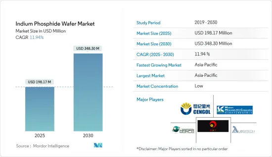
リン化インジウムウエハ市場規模は、2025年に1億9,817万米ドルと推定され、予測期間中(2025年~2030年)のCAGRは11.94%で、2030年には3億4,830万米ドルに達すると予測されています。
リン化インジウム(InP)は、高効率レーザ、変調器、高感度光検出器を生み出す特性を持っています。また、レーザー信号を生成し、その信号を電子形態に変換して識別することもできます。これらは、企業ネットワークやデータセンター、長距離光ファイバー接続、3G、5G、LTE基地局の無線接続、衛星通信などに使用されます。このような要件の増加が市場を牽引しています。
主なハイライト
- リン化インジウムウエハは、車載用LiDAR、3Dセンシング、消費者向けウェアラブル、通信分野におけるデータ通信の成長にますます採用されています。これが予測期間中の市場を牽引すると予想されます。また、InPincの主な用途には、5G通信、ライトやレーザーを使用するデータセンター接続、光ファイバーレーザーと検出器、軍事通信や5G通信で使用されるシリコンフォトニクス、RFアンプ、スイッチ、健康における赤外線サーマルイメージングなどがあります。
- オプトエレクトロニクスデバイスとして知られる電子部品は、光を検出し調整します。オプトエレクトロニックデバイスは、電気情報を赤外線や可視光エネルギーに変換したり、その逆を行ったりします。オプトエレクトロニクスは、太陽光発電、光ファイバー通信システム、モニターおよび制御回路、電気眼球などに利用されています。光電子部品は、量子カスケード・レーザーや誘導放出用注入レーザー・ダイオードに使用されています。LEDとイメージセンサーは、デジタル画像システム、パッケージング、安全アプリケーションに利用されています。
- 2020年11月に発表されたエリクソン・モビリティ・レポートによると、世界のモバイル・データ・トラフィックは2020年末までに月間約51EB(エクサバイト)に達すると推定されています。これはほぼ4.5倍に成長し、2026年には月間226EBに達すると予測されています。この数字は、60億人以上の人々がスマートフォンやノートパソコン、多数の新しいデバイスを使用して一度に消費するモバイルデータを表しています。
- 半導体のシリコン・ウエハはエレクトロニクス産業の基盤であり、多くのマイクロエレクトロニクス・デバイスの主要部品です。現在の技術状況の進歩、電子機器の可動性、デジタル化に伴い、これらのアイテムは幅広いデバイスで使用されるようになっています。また、小型のガジェットが必要とされるようになった結果、1つのデバイスからの追加機能への要求が劇的に高まり、シリコンウエハの価格を押し上げています。
- COVID-19の大流行により、世界中のほとんどの地域で封鎖が続き、半導体製造装置業界ではいくつかの品目の製造が停止しました。封鎖措置は民生用電子機器の需要を減少させ、半導体セクターに世界の影響を与えました。自動車の世界の需要と輸出出荷の継続的な減少は、半導体市場に否定的な影響を引き起こし、現在、半導体製造装置の需要を減速させています。
リン化インジウムウエハ市場動向
市場を牽引するコンシューマー・エレクトロニクス分野
- 開発動向の一つであるウェアラブル技術は、エレクトロニクスを日常活動に統合し、体のどの部分にも装着できる機能でライフスタイルの変化に対応します。インターネットへの接続や、ネットワークとデバイス間のデータ交換オプションの提供といった動向が、ウェアラブル技術の動向につながっています。
- シスコシステムズによると、世界で接続されるウェアラブルデバイスの数は3年間で倍増し、2016年の3億2,500万台から2019年には7億2,200万台に増加します。2022年には10億台を超えると予測されています。
- さらに、総務省(日本)によると、2021年時点で日本の世帯の7%以上がウェアラブル端末を所有しています。ウェアラブル端末の世帯普及率は、調査期間(2014年~2021年)を通して着実に上昇し、2014年の0.5%から2020年には5%に上昇しました。
- 世界各地で都市化率が上昇していることから、1つのデバイスで複数の機能を利用できたり、タイムスケジュールを利用できたりするなど、消費者の要求に応える能力を備えた、先進的で審美的に魅力的な製品に対する需要が高まっています。さらに、世界中の膨大なミレニアル世代は、通常の勤務時間の追跡や贅沢な基準に対する支出能力の増加により、スマートウォッチをいち早く採用しています。
- 例えば、エリクソンによると、世界のスマートフォン契約数は2020年の59億2,400万台から2021年には62億5,900万台に急増しました。2027年には76億9,000万台に達すると推定されています。
- さらに、ノキアの年次モバイル・ブロードバンド指数レポート2022によると、4G対応機器のエコシステムの拡大が、4G加入者とデータ消費の伸びを牽引しています。インドは2021年に、3,000万台の5G端末を含む1億6,000万台以上のスマートフォンの出荷台数で過去最高を記録し、アクティブな4G対応端末は80%を超え、アクティブな5G対応端末は1,000万台を超えました。また、ノキアのレポートでは、2025年までにスマートフォンユーザーの60~75%まで普及が進むと予測しています。
アジア太平洋が急成長市場になる見込み
- アジア太平洋は、TSMCやサムスン電子などの大手企業を擁し、半導体鋳造において世界的に大きなシェアを占めています。台湾、韓国、日本、中国もこの地域で大きなシェアを占めています。米国半導体産業協会(SIA)によると、1990年から2020年にかけて、世界のウエハファブ設置能力における米国のシェアは常に低下しています。同じ期間に、アジアでは新しい半導体工場が急速に開発され、現在では世界の生産能力のかなりの割合を占めるまでになりました。
- 中国は非常に野心的な半導体アジェンダを掲げています。1,500億米ドルの資金を背景に、同国は国内IC産業を発展させ、より多くのチップを製造することを計画しています。香港、中国、台湾を含む大中華圏は、地政学的にホットスポットです。米国と中国の貿易戦争は、主要プロセス技術が集中するこの地域の緊張をさらに高め、多くの中国企業は半導体鋳造工場への投資を余儀なくされています。
- 2021年3月に発表された中国の2021~2025年の新5カ年計画では、基礎研究の強化が重要な優先課題であると定められました。中央政府による基礎研究への支出は2021年に11%増加する見込みで、研究開発投資全体の計画である7%やGDP成長率の目標である6%を大きく上回りました。半導体は、資金と資源の面で優先される7つの分野の1つに指定されました。設計に携わる企業は、コンピューティング、ストレージ、ネットワーク接続、電力管理など、電子機器を機能させる重要なタスクを実行するナノメートルスケールの集積回路を開発します。旺盛なチップ需要により、2021年には利益は2倍以上になると推定されています。中国の大手半導体鋳造工場は、2022年の能力開発のために過去最高額を確保しました。今年、Semiconductor Manufacturing International Corp(SMIC)は資本支出に50億米ドルを確保し、2021年の45億米ドルから増加しました。
- 中国は7nmチップ生産の自立に大きく近づいています。中国は7nmチップ製造プロセスで飛躍的な進歩を遂げ、海外の装置や材料ベンダーへの依存を減らす努力の中で、製造プロセスのいくつかのセグメントでツールやノウハウを開発していると報じられています。
- 研究・提携の著しい拡大は、市場成長率をさらに押し上げます。例えば、LioniXInternational(LXI)とInstitute of Microelectronics Chinese Academy of Science(IMECAS)は、積極的に機能をサポートし、両方のプラットフォームを提供することで、フォトニック集積回路(PIC)プラットフォームのパートナーシップを拡大することに合意しました。PICにおいて重要なプラットフォームには、SOI(Silicon On Insulator)、InP(Indium Phosphide)、窒化シリコンベースのTriPleXplatformがあります。これらのプラットフォームは、マルチ・プロジェクト・ウエハ(MPW)アクセスを通じて入手可能です。
リン化インジウムウエハ産業概要
リン化インジウムウエハ製造分野では、大手メーカーの存在感が高まっており、予測期間中に競争企業間の敵対関係が激化すると予想されます。JX日鉱日石金属やパワーウェイ・アドバンスト・マテリアルのような市場の既存企業は、市場全体にかなりの影響を与えています。
- 2022年3月:インテルはドイツに2つ目のチップ製造拠点「メガファブ」を新設する計画を明らかにしました。さらに2021年8月、ACM Research Inc.はベベルエッチング製品を発売し、ACMのウェットツールの包括的な提供をさらに拡大しました。このツールは、後続のプロセス工程におけるエッジ汚染の影響を最小限に抑え、チップ製造の歩留まりを向上させる。
- 2022年2月:カナダ政府は、カナダの半導体およびフォトニクス産業への多額の投資を発表しました。2億4,000万カナダドルの投資により、カナダはフォトニクスの世界的リーダーとしての役割を固め、半導体の開発と製造を強化します。カナダでは、国内外の半導体企業100社以上がマイクロチップの研究開発に取り組んでいます。化合物半導体、微小電気機械システム(MEMS)、先進パッケージングなどの分野では、30以上の応用研究所と5つの商業施設があります。
その他の特典:
- エクセル形式の市場予測(ME)シート
- 3ヶ月間のアナリスト・サポート
目次
第1章 イントロダクション
- 調査の前提条件と市場定義
- 調査範囲
第2章 調査手法
第3章 エグゼクティブサマリー
第4章 市場洞察
- 市場概要
- 業界の魅力度-ポーターのファイブフォース分析
- 供給企業の交渉力
- 買い手/消費者の交渉力
- 新規参入業者の脅威
- 代替品の脅威
- 競争企業間の敵対関係
- 産業バリューチェーン分析
- 技術スナップショット
- COVID-19の業界への影響評価
第5章 市場力学
- 市場促進要因
- 光電子デバイスの使用の増加
- データ通信ビジネスと5Gの成長
- 市場抑制要因
- 他の代替品との競合
第6章 市場セグメンテーション
- 直径別
- 50.8 mmまたは2インチ
- 76.2mmまたは3インチ
- 100 mmまたは4インチ以上
- エンドユーザー産業別用途
- コンシューマー・エレクトロニクス
- 通信機器
- 医療
- その他のエンドユーザー産業
- 地域別
- 北米
- 欧州
- アジア太平洋
- 世界のその他の地域
第7章 競合情勢
- 企業プロファイル
- AXT Inc.
- Wafer World Inc.
- Logitech Ltd.
- Western Minmetals(SC)Corporation
- Century Goldray Semiconductor Co. Ltd
- Semiconductor Wafer Inc.
- Ding Ten Industrial Inc.
- Sumitomo Electric Semiconductor Materials Inc.(Sumitomo Electric Industries Ltd)
- Xiamen Powerway Advanced Material Co. Ltd
- JX Nippon Mining & Metals Corporation(Eneos Holdings Inc.)
第8章 投資分析
第9章 市場機会と今後の動向
The Indium Phosphide Wafer Market size is estimated at USD 198.17 million in 2025, and is expected to reach USD 348.30 million by 2030, at a CAGR of 11.94% during the forecast period (2025-2030).
Indium phosphide (InP) has properties that produce highly efficient lasers, modulators, and sensitive photodetectors. It can also generate laser signals and convert and identify those signals back to the electronic form. These are used for company networks and data centers, long-haul optical fiber connections over far distances, wireless connections for 3G, 5G, and LTE base stations, and satellite communication. The growth in such requirements is driving the market.
Key Highlights
- Indium phosphide wafers are increasingly adopted in the manufacture of LiDAR for automotive, 3D sensing, consumer wearables, and the growth in datacom in the telecommunication sector. This is expected to drive the market during the forecast period. In addition, some of the major applications of InPinclude 5G communications, data center connectivity that uses lights and lasers, fiber optic lasers and detectors, silicon photonics, RF amplifiers, and switches used in military and 5G communications, and infrared thermal imaging in health.
- Electronic components known as optoelectronic devices detect and regulate light. They convert electrical information into infrared or visible energy and vice versa. It is utilized in photovoltaic power supply, optical fiber communication systems, monitor and control circuits, and electric eyes. Optoelectronic components are used in quantum cascade lasers and injection laser diodes for stimulated emission. LEDs and image sensors are utilized in digital imaging systems, packaging, and safety applications.
- According to the Ericsson Mobility Report published in November 2020, the global mobile data traffic was estimated to reach around 51 EB (exabytes) per month by the end of 2020. This was projected to grow by a factor of almost 4.5 to reach 226 EB per month in 2026. This figure represents the mobile data that will be consumed by greater than 6 billion people using smartphones, laptops, and a multitude of new devices at a time.
- The semiconductor silicon wafer serves as the foundation of the electronics industry and is the main component of many microelectronic devices. With the current advances in the technology landscape, electronic mobility, and digitalization, these items are finding use in a wide range of devices. The requirement for additional capability from a single device has also grown dramatically as a result of the need for small-sized gadgets, which boosts the price of the silicon wafer.
- The COVID-19 pandemic has halted the manufacturing of several items in the semiconductor production equipment industry owing to the continued lockdown in most regions across the world. Lockdown measures reduced the demand for consumer electronic gadgets, which had a global impact on the semiconductor sector. The continued decline in worldwide demand and export shipments for automobiles caused a negative impact on the semiconductor market, which is currently slowing down the demand for semiconductor manufacturing equipment.
Indium Phosphide Wafer Market Trends
Consumer Electronics Segment Expected to Drive the Market
- Wearable technology, a developing trend, integrates electronics into daily activities and addresses the changing lifestyles with the ability to be worn on any part of the body. Factors such as the ability to connect to the internet and provide data exchange options between a network and a device are leading to the trend of wearable technology.
- According to Cisco Systems, the number of connected wearable devices globally has doubled in the span of three years, increasing from 325 million in 2016 to 722 million in 2019. The number of devices is forecasted to be over 1 billion by 2022.
- Further, according to the Ministry of Internal Affairs and Communications (Japan), as of 2021, over 7% of households in Japan owned a wearable device. The household penetration rate of wearable devices steadily increased throughout the surveyed period (2014-2021), rising from 0.5% in 2014 to 5% in 2020.
- The rising rates of urbanization in various parts of the world have driven the demand for advanced, aesthetically appealing products that possess the ability to serve the consumers' requirements better, such as multiple features in one device and time schedules. Moreover, the vast millennial population across the globe has been quick to adopt smartwatches, owing to the increased spending ability on their regular work hours tracking and luxury standards.
- For instance, according to Ericsson, the number of smartphone subscriptions worldwide witnessed an upsurge from 5,924 million in 2020 to 6,259 million in 2021. The number is estimated to reach 7,690 million in 2027.
- Further, according to the Nokia annual mobile broadband index report 2022, the growing ecosystem of 4G-capable devices is driving the growth in 4G subscribers and data consumption. India recorded the highest-ever shipment of over 160 million smartphones, including 30 million 5G devices, in 2021, with active 4G capable devices crossing 80% and the number of active 5G capable devices crossing 10 million. The Nokia report also forecasted that user adoption will increase to 60-75% of the smartphone user base by 2025.
Asia-Pacific Expected to be the Fastest-growing Market
- The Asia-Pacific region commands a prominent share of semiconductor foundries globally, with major companies such as TSMC and Samsung Electronics. Taiwan, South Korea, Japan, and China have a significant market share in the region. According to the US Semiconductor Industry Association (SIA), the US share of the global installed wafer fab capacity constantly declined from 1990 to 2020. During the same period, Asia saw a meteoric rise in developing new fabs to the point where it now accounts for a significant share of the world's capacity.
- China has a very ambitious semiconductor agenda. Backed by USD 150 billion in funding, the country is developing its domestic IC industry and plans to make more of its chips. Greater China, which encompasses Hong Kong, China, and Taiwan, is a geopolitical hotspot. The US-China trade war is compounding tensions in an area where all the leading process technology is located, forcing many Chinese companies to invest in their semiconductor foundries.
- China's new five-year plan for 2021-2025, announced in March 2021, established that boosting basic research was a critical priority. The central government's spending on basic research was expected to increase by 11% in 2021, well above the 7% planned for the overall R&D investment and the 6% target for GDP growth. Semiconductors were designated as one of the seven areas that will be given priority in terms of funding and resources. Firms involved in design develop nanometer-scale integrated circuits that perform the critical tasks that make electronic devices work, such as computing, storage, network connectivity, and power management. The profit was estimated to more than double in 2021 because of the robust chip demand. China's leading semiconductor foundry set aside a record sum for capacity development in 2022. This year, Semiconductor Manufacturing International Corp (SMIC) set aside USD 5 billion for capital spending, up from USD 4.5 billion in 2021.
- China is moving significantly closer to self-reliance in 7 nm chip production. China has made breakthroughs in its 7 nm chip-making process, reportedly developing tools and know-hows for several segments of the manufacturing process amid efforts to reduce reliance on foreign equipment and material vendors.
- The significant research and partnership growth further bolsters the market growth rate. For instance, LioniXInternational (LXI) and the Institute of Microelectronics Chinese Academy of Science (IMECAS) agreed to expand their Photonic Integrated Circuit (PIC) platform partnership by actively supporting the functionality and offering both platforms. The critical platforms in the PIC landscape include Silicon On Insulator (SOI), Indium Phosphide (InP), and the silicon nitride-based TriPleXplatform. These platforms are available through Multi-Project Wafer (MPW) access.
Indium Phosphide Wafer Industry Overview
The growing presence of large manufacturers in the indium phosphide wafer manufacturing sector is expected to intensify competitive rivalry during the forecast period. Market incumbents, such as JX Nippon Mining & Metals Corporation and Powerway Advanced Material Co. Ltd, considerably influence the overall market.
- March 2022: Intel revealed plans for a second new 'Megafab," a chipmaking site in Germany, with an expected USD 88 billion in investments across several European countries. Further, in August 2021, ACM Research Inc. launched its Bevel Etch product, which further expanded ACM's comprehensive offering of wet tools. This tool minimizes the impact of edge contamination for subsequent process steps and improves chip manufacturing yield.
- February 2022: The Government of Canada announced a significant investment in the Canadian semiconductor and photonics industries. The investment of CAD 240 million will help solidify Canada's role as a global leader in photonics and will bolster the development and manufacturing of semiconductors. Over 100 domestic and international semiconductor companies work on microchip research and development in Canada. There are over 30 applied research laboratories and five commercial facilities for areas including compound semiconductors, microelectromechanical systems (MEMS), and advanced packaging.
Additional Benefits:
- The market estimate (ME) sheet in Excel format
- 3 months of analyst support
TABLE OF CONTENTS
1 INTRODUCTION
- 1.1 Study Assumptions and Market Definition
- 1.2 Scope of the Study
2 RESEARCH METHODOLOGY
3 EXECUTIVE SUMMARY
4 MARKET INSIGHTS
- 4.1 Market Overview
- 4.2 Industry Attractiveness - Porter's Five Forces Analysis
- 4.2.1 Bargaining Power of Suppliers
- 4.2.2 Bargaining Power of Buyers/Consumers
- 4.2.3 Threat of New Entrants
- 4.2.4 Threat of Substitute Products
- 4.2.5 Intensity of Competitive Rivalry
- 4.3 Industry Value Chain Analysis
- 4.4 Technology Snapshot
- 4.5 Assessment of the Impact of COVID-19 on the Industry
5 MARKET DYNAMICS
- 5.1 Market Drivers
- 5.1.1 Increasing Use of Optoelectronic Devices
- 5.1.2 Growth of Datacom Business and 5G
- 5.2 Market Restraints
- 5.2.1 Competition from Other Substitutes
6 MARKET SEGMENTATION
- 6.1 By Diameter
- 6.1.1 50.8 mm or 2 "
- 6.1.2 76.2 mm or 3 "
- 6.1.3 100 mm or 4" and Above
- 6.2 By End-user Industry Application
- 6.2.1 Consumer Electronics
- 6.2.2 Telecommunications
- 6.2.3 Medical
- 6.2.4 Other End-user Industry Applications
- 6.3 By Geography
- 6.3.1 North America
- 6.3.2 Europe
- 6.3.3 Asia-Pacific
- 6.3.4 Rest of the world
7 COMPETITIVE LANDSCAPE
- 7.1 Company Profiles
- 7.1.1 AXT Inc.
- 7.1.2 Wafer World Inc.
- 7.1.3 Logitech Ltd.
- 7.1.4 Western Minmetals (SC) Corporation
- 7.1.5 Century Goldray Semiconductor Co. Ltd
- 7.1.6 Semiconductor Wafer Inc.
- 7.1.7 Ding Ten Industrial Inc.
- 7.1.8 Sumitomo Electric Semiconductor Materials Inc. (Sumitomo Electric Industries Ltd)
- 7.1.9 Xiamen Powerway Advanced Material Co. Ltd
- 7.1.10 JX Nippon Mining & Metals Corporation (Eneos Holdings Inc.)
