
|
市場調査レポート
商品コード
1851280
アドバンストパッケージング:市場シェア分析、産業動向、統計、成長予測(2025年~2030年)Advanced Packaging - Market Share Analysis, Industry Trends & Statistics, Growth Forecasts (2025 - 2030) |
||||||
カスタマイズ可能
適宜更新あり
|
|||||||
| アドバンストパッケージング:市場シェア分析、産業動向、統計、成長予測(2025年~2030年) |
|
出版日: 2025年07月11日
発行: Mordor Intelligence
ページ情報: 英文 126 Pages
納期: 2~3営業日
|

概要
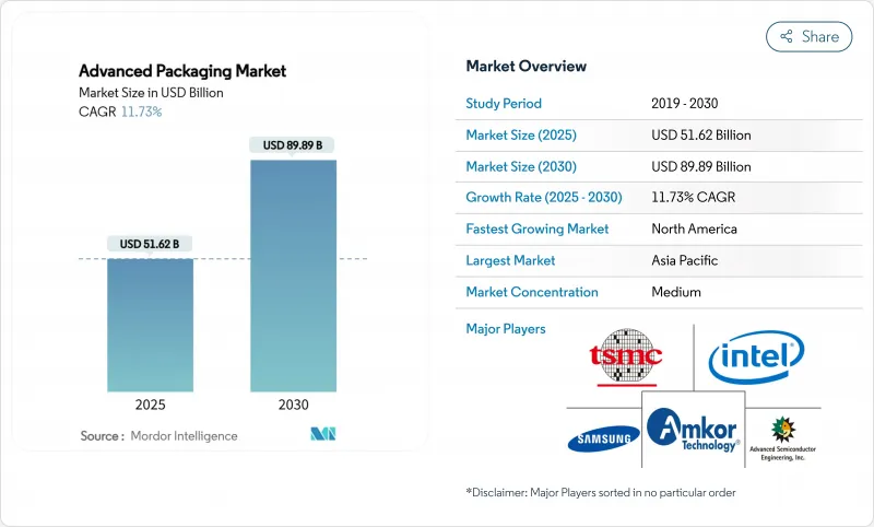
アドバンストパッケージング市場規模は2025年に516億2,000万米ドルとなり、CAGR 11.73%で拡大し、2030年には898億9,000万米ドルに達すると予測されています。
従来のパッケージでは熱や相互接続の限界を超える人工知能(AI)プロセッサにヘテロジニアス集積が不可欠となったため、需要は以前の予測を上回りました。これを受けて、集積デバイスメーカー(IDMs)および半導体組立・テストアウトソーシング(OSAT)プロバイダーは設備投資を加速、一方政府は組立能力を現地化するために多額の奨励金を計上しました。アドバンストパッケージング市場はまた、ガラスコア基板の研究開発、パネルレベル処理の試験運用、ハイパースケールデータセンターにおけるコパッケージ光学部品の急速な採用からも恩恵を受けました。しかし、BTレジン基板の不足とエンジニアの人材不足がタイムリーな生産能力増強の妨げとなり、供給は依然として逼迫しています。AIサプライチェーンをエンド・ツー・エンドで管理するため、鋳造メーカーがパッケージングを内製化し、従来のOSATのマージンが圧迫され、戦略的な専門化が促されたため、競合は激化しました。
世界のアドバンストパッケージング市場の動向と洞察
AIとHPC向けのヘテロジニアス統合に対する需要の高まり
AIワークロードは、従来のパッケージングでは実現できなかった計算密度とメモリ帯域幅を必要とします。TSMCのCoWoSプラットフォームは、チップレットと高帯域幅メモリを単一構造に統合し、主要AIアクセラレータ・ベンダーの間で急速に採用が進んでいます。サムスンのSAINT技術は、ハイブリッドボンディングを使用して同様の目標を達成し、今後予定されているHBM4スタックをサポートすることで、社内のアドバンストパッケージングの戦略的価値を強調しています。熱インターフェース材料、特殊基板、アクティブインターポーザは、パッケージコストを半導体全体の15~20%に引き上げ、主流CPUの5~8%から上昇させました。その結果、アドバンストパッケージングのキャパシティは、AIシステムの市場投入までの時間を決定する上で、最先端ファブと同様に極めて重要になりました。したがって、アドバンストパッケージング市場は、前工程の移行に遅れることなく、むしろ連動して成長しました。
コンシューマ機器の小型化がWLP採用を後押し
スマートフォン、ウェアラブル端末、ヒアラブル端末では、薄型化と機能密度の向上が常に求められています。ファンアウト・ウエハーレベル・パッケージング(FOWLP)は、0.5mm以下の超薄型パッケージに複数のダイを内蔵することを可能にし、熱性能を損なうことなくフラッグシップ・モバイル・プロセッサをサポートします。ファンインWLPからFOWLPへの移行により、アンダーフィル、ワイヤーボンディング、ラミネート基板が不要になったため、システム全体のコストが最大25%削減されました。小型化はまた、寸法が生命にかかわる埋め込み型医療用電子機器にも進み、リードレス・ペースメーカーはWLPの恩恵を受けて、厳しい信頼性目標を満たしながらデバイスサイズを93%削減しました。その結果、消費者需要と医療需要は、PC最終市場の周期的変動からアドバンストパッケージング市場を隔離する経常的なベースラインを作り出しました。
高い資本集約度が市場参入を制約
2.5Dおよび3Dプロセス用のツーリングには、チャンバー当たり1,000万~1,500万米ドルのコストがかかり、レガシー・ラインの一般的な300万米ドルを大幅に上回る。TSMCは2025年の資本支出に420億米ドルを予算計上しており、そのうちの重要なシェアはアドバンストパッケージングの拡張を対象としています。そのため、小規模なOSATは、急速に縮小する製品ライフサイクルにわたって投資を償却するのに苦労し、ニッチな専門化や防衛的な合併を促しました。高いハードルレートは、ティアワン・プロバイダーと地域フォロワーとの間の技術格差を広げ、2024-2026年のアドバンストパッケージング市場における新たな生産能力を減衰させました。
セグメント分析
フリップチップパッケージは、2024年の売上高49.0%で首位を維持し、大量生産される消費者向けおよび産業向けアプリケーションに支えられています。しかし、2.5D/3Dコンフィギュレーションは、AIアクセラレータがフリップチップの限界を超えたロジックーメモリ間の近接性を要求していることから、13.2%のCAGR見通しを達成し、最も速い伸びを示しました。2.5D/3Dソリューションのアドバンストパッケージング市場規模は、2030年までに341億米ドルに達し、プラットフォーム全体の収益の38%に相当すると予測されています。
サムスンのSAINTプラットフォームは、10µm以下のハイブリッド・ボンドを達成し、ワイヤ・ボンド・スタックと比較して、信号レイテンシを30%削減し、サーマル・ヘッドルームを40%拡大した。TSMCのCoWoSは、2025年に3つのラインを増設し、12カ月のバックログをクリアしました。組み込み型パッケージはスペースに制約のある車載領域に適しており、ファンアウト型WLPは5G基地局やミリ波レーダーの設計に適しています。これらのダイナミクスを総合すると、2.5D/3Dパッケージングが次世代デバイスのロードマップの中心に組み込まれ、アドバンストパッケージング市場内の主要なバリュードライバーとしての役割が保証されました。
コンシューマーエレクトロニクスは2024年の出荷の40.0%を吸収したが、その成長は1桁台に停滞しました。これとは対照的に、自動車とEVの需要はCAGR 12.4%で拡大し、2030年までにアドバンストパッケージング市場のシェアを18%に引き上げると予測されています。車載エレクトロニクスのアドバンストパッケージング市場規模は、予測期間末までに160億米ドルを超えると予測されます。
EVトラクション・インバータ、オンボード・チャージャー、ドメイン・コントローラは、現在、車載グレードのファンアウト、ダブルサイド冷却パワーモジュール、オーバーモールド・システム・イン・パッケージ(SiP)アセンブリを指定しています。データセンターインフラストラクチャは、もう一つの高成長ニッチ分野となった:AIサーバーは、電力密度が1,000W/cm2に達するアドバンストパッケージングを利用しており、革新的なサーマルリッドとアンダーフィルケミストリーを必要としています。一方、ヘルスケアでは、生体適合性コーティングと密閉型エンクロージャーが必要とされ、その特性から平均販売価格は割高となり、安定した買い替え需要があります。これらのセグメント動向は、収益源を多様化し、アドバンストパッケージング市場の周期的なスマートフォンのリフレッシュサイクルへの依存を低減しています。
アドバンストパッケージング市場は、パッケージングプラットフォーム(フリップチップ、エンベデッドダイ、ファンインWLPなど)、エンドユーザー産業(コンシューマーエレクトロニクス、自動車およびEV、データセンターおよびHPCなど)、デバイスアーキテクチャ(2D IC、2.5Dインターポーザー、3D IC)、相互接続技術(はんだバンプ、銅ピラー、ハイブリッドボンド)、地域(北米、南米、欧州、アジア太平洋、中東アフリカ)で区分されます。
地域別分析
アジア太平洋は、台湾、韓国、中国本土がフロントエンド工場と基板サプライヤーの大部分を占めているため、2024年の売上高の75.0%を生み出しました。TSMCは1,650億米ドルの米国投資を発表したが、これは台湾拠点の移転ではなく多角化戦略を反映したものであり、アジアが中期的にリーダーシップを維持することを保証するものです。中国国内のOSATは売上高が2桁の伸びを示し、自動車用パッケージングにも進出したが、極端紫外線(EUV)ツールの規制が厳しく、最先端ウエハーファブプロセスへの進出は制限されました。
北米は、CHIPS法の優遇措置によりCAGR 12.5%の急成長地域として浮上しました。Amkorの20億米ドル規模のアリゾナ拠点は、2027年に全面稼働するとバンプ、ウェーハレベル、パネルレベルのラインを統合し、米国のシステムインテグレーターの近くで初の大規模アウトソーシングオプションを提供する予定です。インテル、アップル、エヌビディアは、地政学的な供給中断のリスクを回避するため、この生産能力の一部を事前に予約し、これまで東アジアのOSATに流れていた重要な生産量を転換しました。その結果、アドバンストパッケージング市場には、大量のAI製品をサポートできる信頼できる北米の供給ノードが含まれるようになりました。
onsemiのチェコ拠点は、車載電源用シリコンカーバイドデバイスに取り組み、現地OEMの電動化目標に合致しました。ドイツのフラウンホーファー研究機構はパネルレベルの研究を主導したが、メーカー各社はグリーンフィールドのメガサイトコミットメントには慎重でした。一方、シンガポールはハブの役割を強化しました。マイクロンのHBM工場とKLAのプロセス制御拡張により、AIメモリと計測を1つの管轄下でサポートする垂直的に首尾一貫したエコシステムが構築されました。インドでは、50%の資本コスト負担スキームが導入され、中期的なアップサイドが期待されるもの、人材の確保次第ではあるもの、アドバンストパッケージングパイロットの提案が集まりました。
これらの開拓は、システムOEMの地理的リスクを分散させ、アドバンストパッケージング市場のバランスを調整しました。それでも、アジア太平洋地域は2030年に60%以上のシェアを維持すると予測されています。これは、既存のインフラ、供給クラスター、規模の経済が、依然として新規参入企業を上回っているからです。
その他の特典:
- エクセル形式の市場予測(ME)シート
- 3ヶ月間のアナリストサポート
よくあるご質問
目次
第1章 イントロダクション
- 調査の前提条件と市場の定義
- 調査範囲
第2章 調査手法
第3章 エグゼクティブサマリー
第4章 市場情勢
- 市場概要
- マクロ経済要因の影響
- 市場促進要因
- AIとHPCのためのヘテロジニアス統合に対する需要の高まり
- 消費者向け機器の小型化がWLP採用を後押し
- 政府の半導体補助金(例:CHIPS、EUチップ法)
- EVパワーエレクトロニクスの信頼性ニーズ(先進パワーパッケージ)
- パネルレベルパッケージングを可能にする新たなガラスコア基板
- ハイパースケールデータセンターにおけるコパッケージドオプティクスの需要
- 市場抑制要因
- アドバンストパッケージングラインの資本集約度の高さ
- アウトソーシングのマージンを圧迫する業界再編
- BTレジン基板の生産能力ボトルネック
- 高度組み立て人材の不足
- バリューチェーン分析
- 規制情勢
- テクノロジーの展望
- ポーターのファイブフォース分析
- 新規参入業者の脅威
- 買い手の交渉力
- 供給企業の交渉力
- 代替品の脅威
- ライバルの激しさ
- 投資分析
第5章 市場規模と成長予測
- パッケージング・プラットフォーム別
- フリップチップ
- 組み込み型
- ファンインWLP
- ファンアウトWLP
- 2.5D/3D
- エンドユーザー業界別
- コンシューマーエレクトロニクス
- 自動車・EV
- データセンターとHPC
- 産業用およびIoT
- ヘルスケア/ 医療技術
- デバイスアーキテクチャ別
- 2DIC
- 2.5Dインターポーザー
- 3D IC(TSV/ハイブリッド・ボンド)
- 相互接続技術別
- はんだバンプ
- 銅柱
- ハイブリッドボンド
- 地域別
- 北米
- 米国
- カナダ
- メキシコ
- 南米
- ブラジル
- アルゼンチン
- その他南米
- 欧州
- ドイツ
- フランス
- 英国
- イタリア
- オランダ
- ロシア
- その他欧州地域
- アジア太平洋地域
- 中国
- 台湾
- 韓国
- 日本
- シンガポール
- マレーシア
- インド
- その他アジア太平洋地域
- 中東・アフリカ
- 中東
- イスラエル
- アラブ首長国連邦
- サウジアラビア
- トルコ
- その他中東
- アフリカ
- 南アフリカ
- ナイジェリア
- その他アフリカ
- 北米
第6章 競合情勢
- 市場集中度
- 戦略的動向
- 市場シェア分析
- 企業プロファイル
- Amkor Technology, Inc.
- Taiwan Semiconductor Manufacturing Company Limited
- Advanced Semiconductor Engineering, Inc.
- JCET Group Co., Ltd.
- Samsung Electronics Co., Ltd.
- Intel Corporation
- Chipbond Technology Corporation
- ChipMOS Technologies Inc.
- Powertech Technology Inc.
- TongFu Microelectronics Co., Ltd.
- Nepes Corporation
- STATS ChipPAC Pte. Ltd.
- Siliconware Precision Industries Co., Ltd.
- UTAC Holdings Ltd.
- Walton Advanced Engineering, Inc.
- Xintec Inc.
- Tianshui Huatian Technology Co., Ltd.
- King Yuan Electronics Co., Ltd.
- Signetics Corporation
- GlobalFoundries Inc.
- Semiconductor Manufacturing International Corporation
- SFA Semicon Co., Ltd.
- Nantong Fujitsu Microelectronics Co., Ltd.
- Hana Micron Inc.
- Unisem(M)Berhad

