|
|
市場調査レポート
商品コード
1698495
半導体後工程装置市場:将来予測 (2025年~2030年)Semiconductor Back-End Equipment Market - Forecasts from 2025 to 2030 |
||||||
|
|||||||
カスタマイズ可能
|
|||||||

| 半導体後工程装置市場:将来予測 (2025年~2030年) |
|
出版日: 2025年03月24日
発行: Knowledge Sourcing Intelligence
ページ情報: 英文 155 Pages
納期: 即日から翌営業日
|

全表示
- 概要
- 目次
半導体後工程装置市場はCAGR 6.89%で成長し、2025年の市場規模1,130億600万米ドルから2030年には1,576億9,300万米ドルに達すると予測されます。
ノートパソコン、デジタルカメラ、スマートフォンなどの電子製品において、小型デバイスの需要が高まり、機能が進化していることから、市場の拡大が見込まれています。集積回路(IC)の設計は高度に複雑化しており、ICを製造するためにはより多くの半導体製品を導入する必要があるため、半導体後工程装置の需要は着実に増加しています。半導体がIC開発に使われるのは、コストを下げ、量産を早め、完成品の運用価値を高めるためです。
市場動向:
- 半導体需要の急増:半導体の世界需要は、さまざまな産業分野での用途拡大に牽引され、増加の一途をたどっています。新興企業や若手企業は、製品開発や生産のニーズを満たすため、ODM(Original Design Manufacturers)やOSAT(Outsourced Semiconductor Assembly and Test)プロバイダーを利用するようになっています。世界各国の政府は、海外サプライヤーへの依存を減らすため、現地での半導体製造を優先し、既存メーカーからの直接投資を奨励し、支援的な規制枠組みを提供しています。例えば、半導体産業協会(SIA)は、2024年の世界半導体売上高は6,276億米ドルに達し、2023年の5,268億米ドルから19.1%増加すると報告しています。
- 製造業におけるニーズの高まり:半導体製造装置は、半導体ウエハー、ICチップ、メモリーチップ、回路、その他のコンポーネントの製造に不可欠です。シリコンウエハー製造装置は製造の初期段階において重要な役割を果たし、ウエハー処理装置(フォトリソグラフィ装置、エッチング装置、化学気相成長装置、測定装置、プロセス/品質管理装置など)はワークフローに不可欠です。半導体後工程装置の市場は、さまざまなエンドユーザー用途におけるディスクリートデバイス、パワー半導体、ハイパワーモジュールの需要増加により拡大が見込まれています。さらに、複数の半導体機能を1つのチップに集積するトレンドは、消費者がより小型でコンパクトな製品を好むようになり、後工程の装置は主にこれらのコンポーネントを統合チップに組み立てるために使用されています。
- アジア太平洋地域での急成長:アジア太平洋地域の半導体後工程装置市場は、予測期間中に急成長を遂げる見込みです。この急成長の原動力となるのは、国内大手サプライヤーの戦略的投資と、同地域で確立された半導体産業の拡大です。チップ消費量の増加に伴い、アジア太平洋半導体市場は今後4年間で南北アメリカの3倍の規模になると予測されています。5G技術の展開がこの地域の半導体チップ需要をさらに増幅し、製造装置市場の成長に拍車をかけています。この5Gの進歩により、世界中のデジタルインフラが大幅に強化されると期待されています。
当レポートで取り上げている主要企業には、ASML Holding N.V.、Applied Materials、Lam Research、東京エレクトロン、Rapidus Corporation、KLA Corporation、Onto Innovation Inc.などがあります。
当レポートの主な利点
- 洞察に満ちた分析:顧客セグメント、政府政策と社会経済要因、消費者の嗜好、産業別、その他のサブセグメントに焦点を当て、主要地域だけでなく新興地域もカバーする詳細な市場考察を得ることができます。
- 競合情勢:世界の主要企業が採用している戦略的作戦を理解し、適切な戦略による市場浸透の可能性を理解することができます。
- 市場促進要因と将来動向:ダイナミックな要因と極めて重要な市場動向、そしてそれらが今後の市場展開をどのように形成していくかを探ります。
- 行動可能な提言:ダイナミックな環境の中で、新たなビジネスストリームと収益を発掘するための戦略的意思決定に洞察を活用します。
- 幅広い利用者に対応:新興企業、研究機関、コンサルタント、中小企業、大企業にとって有益で費用対効果が高いです。
どのような用途で利用されていますか?
業界・市場考察、事業機会評価、製品需要予測、市場参入戦略、地理的拡大、設備投資決定、規制の枠組みと影響、新製品開発、競合の影響
分析範囲
- 過去のデータ(2022~2024年)と予測データ (2025~2030年)
- 成長機会、課題、サプライチェーンの展望、規制枠組み、顧客行動、動向分析
- 競合企業のポジショニング・戦略・市場シェア分析
- 収益成長率と予測分析:セグメント別・地域別 (国別)
- 企業プロファイリング (戦略、製品、財務情報、主な動向など)
半導体後工程装置市場の内訳:
手順別
- ウエハー検査
- ボンディング
- ダイシング
- 計測
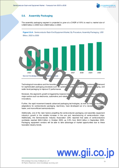
- アセンブリ・パッケージング
地域別
- 南北アメリカ
- 米国
- 欧州・中東・アフリカ
- ドイツ
- オランダ
- その他
- アジア太平洋
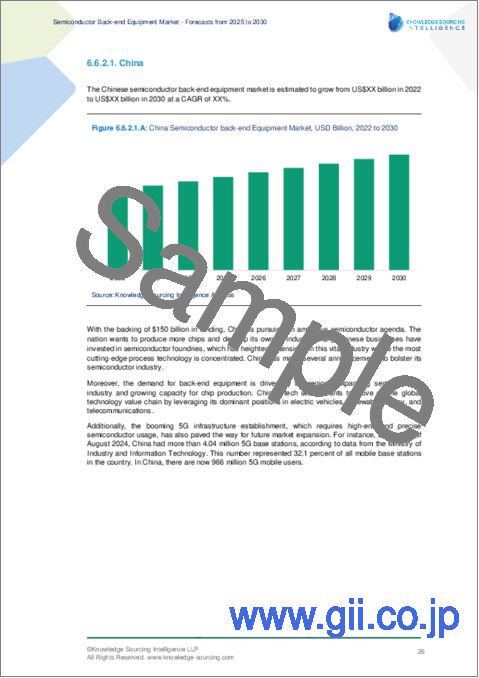
- 中国
- 日本
- 台湾
- 韓国
- その他
目次
第1章 エグゼクティブサマリー
第2章 市場スナップショット
- 市場概要
- 市場の定義
- 分析範囲
- 市場区分
第3章 ビジネス情勢
- 市場促進要因
- 市場抑制要因
- 市場機会
- ポーターのファイブフォース分析
- 業界バリューチェーン分析
- ポリシーと規制
- 戦略的推奨事項
第4章 技術展望
第5章 半導体後工程装置市場:手順別
- イントロダクション
- ウエハー検査
- ボンディング
- ダイシング
- 計測
- アセンブリ・パッケージング
第6章 半導体後工程装置市場:地域別
- イントロダクション
- 南北アメリカ
- 米国
- 欧州、中東・アフリカ
- ドイツ
- オランダ
- その他
- アジア太平洋
- 中国
- 日本
- 台湾
- 韓国
- その他
第7章 競合環境と分析
- 主要企業と戦略分析
- 市場シェア分析
- 企業合併・買収 (M&A)、合意、事業協力
- 競合ダッシュボード
第8章 企業プロファイル
- ASML Holding N.V.
- Applied Materials
- Lam Research
- Tokyo Electron Limited
- Rapidus Corporation
- KLA Corporation
- Onto Innovation Inc.
- SCREEN Holdings Co., Ltd.
- Toshiba Corporation
第9章 付録
- 通貨
- 前提条件
- 基準年と予測年のタイムライン
- 利害関係者にとっての主なメリット
- 分析手法
- 略語
The semiconductor back-end equipment market is expected to grow at a CAGR of 6.89%, reaching a market size of US$157.693 billion in 2030 from US$113.006 billion in 2025.
The market is expected to grow due to the increasing demand for small devices and functional advancements in electronic goods like laptops, digital cameras, smartphones, and others. Since integrated circuit (IC) designs are becoming highly complex and more semiconductor products must be introduced to manufacture ICs, the demand for semiconductor back-end equipment is increasing steadily. Semiconductors are used in IC development because they lower costs, speed up mass production, and increase the operational value of the finished product.
Market Trends:
- Surging Semiconductor Demand: Global demand for semiconductors is on the rise, driven by expanding applications across various industries. Emerging and younger companies are increasingly turning to Original Design Manufacturers (ODMs) and Outsourced Semiconductor Assembly and Test (OSAT) providers to meet their product development and production needs. Governments worldwide are prioritizing local semiconductor manufacturing to lessen dependence on foreign suppliers, encouraging direct investments from established manufacturers and offering supportive regulatory frameworks. For example, the Semiconductor Industry Association (SIA) reported that global semiconductor sales hit US$627.6 billion in 2024, reflecting a 19.1% increase from the US$526.8 billion recorded in 2023.
- Growing Needs in Manufacturing: Semiconductor manufacturing equipment is essential for producing semiconductor wafers, IC chips, memory chips, circuits, and other components. Silicon wafer production equipment plays a key role in the initial stages of manufacturing, while wafer processing tools-such as photolithography machines, etching devices, chemical vapor deposition systems, measurement tools, and process/quality control equipment-are critical to the workflow. The market for semiconductor back-end equipment is expected to grow due to increasing demand for discrete devices, power semiconductors, and high-power modules across various end-user applications. Additionally, the trend of integrating multiple semiconductor functions onto a single chip is gaining traction as consumers favor smaller, compact products, with back-end equipment primarily used for assembling these components into a unified chip.
- Exponential Growth in Asia Pacific: The Asia-Pacific semiconductor back-end equipment market is set to experience rapid growth during the forecast period. This surge is driven by strategic investments from leading domestic suppliers and the expansion of the region's well-established semiconductor industry. With chip consumption on the rise, the Asia-Pacific semiconductor market is projected to triple in size compared to the Americas over the next four years. The rollout of 5G technology has further amplified demand for semiconductor chips in the region, spurring growth in the market for manufacturing equipment. This advancement in 5G is expected to significantly enhance digital infrastructure worldwide.
Some of the major players covered in this report include ASML Holding N.V., Applied Materials, Lam Research, Tokyo Electron Limited, Rapidus Corporation, KLA Corporation, Onto Innovation Inc., among others.
Key Benefits of this Report:
- Insightful Analysis: Gain detailed market insights covering major as well as emerging geographical regions, focusing on customer segments, government policies and socio-economic factors, consumer preferences, industry verticals, and other sub-segments.
- Competitive Landscape: Understand the strategic maneuvers employed by key players globally to understand possible market penetration with the correct strategy.
- Market Drivers & Future Trends: Explore the dynamic factors and pivotal market trends and how they will shape future market developments.
- Actionable Recommendations: Utilize the insights to exercise strategic decisions to uncover new business streams and revenues in a dynamic environment.
- Caters to a Wide Audience: Beneficial and cost-effective for startups, research institutions, consultants, SMEs, and large enterprises.
What do businesses use our reports for?
Industry and Market Insights, Opportunity Assessment, Product Demand Forecasting, Market Entry Strategy, Geographical Expansion, Capital Investment Decisions, Regulatory Framework & Implications, New Product Development, Competitive Intelligence
Report Coverage:
- Historical data from 2022 to 2024 & forecast data from 2025 to 2030
- Growth Opportunities, Challenges, Supply Chain Outlook, Regulatory Framework, and Trend Analysis
- Competitive Positioning, Strategies, and Market Share Analysis
- Revenue Growth and Forecast Assessment of segments and regions including countries
- Company Profiling (Strategies, Products, Financial Information, and Key Developments among others)
Semiconductor Back-End Equipment Market Segmentation:
By Procedure
- Wafer Testing
- Bonding
- Dicing
- Metrology
- Assembly Packaging
By Geography
- Americas
- US
- Europe, the Middle East, and Africa
- Germany
- Netherlands
- Others
- Asia Pacific
- China
- Japan
- Taiwan
- South Korea
- Others
TABLE OF CONTENTS
1. EXECUTIVE SUMMARY
2. MARKET SNAPSHOT
- 2.1. Market Overview
- 2.2. Market Definition
- 2.3. Scope of the Study
- 2.4. Market Segmentation
3. BUSINESS LANDSCAPE
- 3.1. Market Drivers
- 3.2. Market Restraints
- 3.3. Market Opportunities
- 3.4. Porter's Five Forces Analysis
- 3.5. Industry Value Chain Analysis
- 3.6. Policies and Regulations
- 3.7. Strategic Recommendations
4. TECHNOLOGICAL OUTLOOK
5. SEMICONDUCTOR BACK-END EQUIPMENT MARKET BY PROCEDURE
- 5.1. Introduction
- 5.2. Wafer Testing
- 5.3. Bonding
- 5.4. Dicing
- 5.5. Metrology
- 5.6. Assembly Packaging
6. SEMICONDUCTOR BACK-END EQUIPMENT MARKET BY GEOGRAPHY
- 6.1. Introduction
- 6.2. Americas
- 6.2.1. USA
- 6.3. Europe, Middle East, and Africa
- 6.3.1. Germany
- 6.3.2. Netherlandss
- 6.3.3. Others
- 6.4. Asia Pacific
- 6.4.1. China
- 6.4.2. Japan
- 6.4.3. Taiwan
- 6.4.4. South Korea
- 6.4.5. Others
7. COMPETITIVE ENVIRONMENT AND ANALYSIS
- 7.1. Major Players and Strategy Analysis
- 7.2. Market Share Analysis
- 7.3. Mergers, Acquisitions, Agreements, and Collaborations
- 7.4. Competitive Dashboard
8. COMPANY PROFILES
- 8.1. ASML Holding N.V.
- 8.2. Applied Materials
- 8.3. Lam Research
- 8.4. Tokyo Electron Limited
- 8.5. Rapidus Corporation
- 8.6. KLA Corporation
- 8.7. Onto Innovation Inc.
- 8.8. SCREEN Holdings Co., Ltd.
- 8.9. Toshiba Corporation
9. APPENDIX
- 9.1. Currency
- 9.2. Assumptions
- 9.3. Base and Forecast Years Timeline
- 9.4. Key benefits for the stakeholders
- 9.5. Research Methodology
- 9.6. Abbreviations

