|
|
市場調査レポート
商品コード
1114953
電子顕微鏡の世界市場規模、シェア、産業動向分析レポート:タイプ別(走査型、透過型)、用途別(半導体、生命科学、材料科学)、エンドユーザー別、地域別展望・予測、2022年~2028年Global Electron Microscopy Market Size, Share & Industry Trends Analysis Report By Type (Scanning and Transmission), By Application (Semiconductors, Life Sciences, and Material Sciences), By End User, By Regional Outlook and Forecast, 2022 - 2028 |
||||||
|
|
|||||||


| 電子顕微鏡の世界市場規模、シェア、産業動向分析レポート:タイプ別(走査型、透過型)、用途別(半導体、生命科学、材料科学)、エンドユーザー別、地域別展望・予測、2022年~2028年 |
|
出版日: 2022年07月29日
発行: KBV Research
ページ情報: 英文 204 Pages
納期: 即納可能
|
- 全表示
- 概要
- 図表
- 目次
電子顕微鏡の世界市場規模は、2028年には52億米ドルに達し、予測期間中にCAGR7.8%の市場成長率で上昇すると予測されています。
ラスターの各ポイントは、一次電子ビームが表面に近い原子と相互作用した結果、粒子を放出します。低エネルギーの二次電子、高エネルギーの後方散乱電子、X線、そして光子も放出します。これらをさまざまな検出器で集め、その相対的な数からブラウン管上の各類似位置の明るさを計算することができます。最終的な画像は、試料でのラスターの大きさがブラウン管の表示画面よりかなり小さいため、試料の拡大画像となります。二次検出器、後方散乱検出器、X線検出器が適切にセットアップされたSEMは、試料の表面形状、原子組成、免疫標識の分布などを調べることができます。
COVID-19影響分析
COVID-19の発生により、貿易や経済活動は世界中どこでも影響を受けています。自動車や航空宇宙産業向けの小さなソフトウェア産業が被害を受ける一方、ヘルスケアや半導体産業向けの小さなソフトウェア市場は成長すると予想されます。世界のいくつかの国が州をあげてのロックダウンや様々な産業の一時的な閉鎖を宣言した結果、生産や製造に大きな影響を及ぼしています。貿易制限により、需給のミスマッチが深刻化しています。COVID-19の流行は、電子顕微鏡市場向け半導体を製造する企業に、現在も将来も様々な形で影響を与えると思われます。
市場の成長要因
顕微鏡技術の向上
デジタル化、超解像、ライブセルイメージング、ハイスループット技術などは、顕微鏡の技術開発の一例です。これらの進歩は、製品コストや検査コストの低減に寄与しています。最近では、拡張顕微鏡、走査型ヘリウム顕微鏡(SHeM)、多視点顕微鏡、統合顕微鏡システムなど、さまざまな顕微鏡が開発されています。電子顕微鏡とサンプル調製における最も最近の開発の中には、デジタル顕微鏡があります。デジタル画像処理は、画像の解像度と精度が高いため、試料をよりよく観察でき、画像の歪みも少なくなります。また、スライドスキャン装置が完成したことにより、デジタル顕微鏡の普及が加速されました。
倍率と被写界深度の向上
可視光の最も短い波長である約0.4マイクロメートルが、科学者が光学顕微鏡で見ることができる最大のものです。それ以下の大きさのものは光を反射しないので、光を使った装置では見ることができません。原子、分子、ウイルス粒子などがこれにあたる。電子顕微鏡は、可視光線の反射に頼らないので、これらの物体の像を映し出すことができます。電子顕微鏡では、試料に高エネルギーの電子を照射し、その電子が試料で反射・偏向したときの振る舞いを情報として画像化します。
市場阻害要因
専門家の不足
標準的な化合物顕微鏡は、物理学者や研究者が簡単に使えるものですが、高度な顕微鏡が開発されると、訓練を受けた人材が必要になります。例えば、ナノテクノロジー分野で広く使われている原子間力顕微鏡は、化学物質や生物学的化合物の特性を原子や分子のレベルで研究するため、物理学者や技術者が表面物理学や表面分析の分野で深い学際的知識を持つことが必要です。電子顕微鏡は、外部からの磁場や振動で大きなダメージを受ける繊細な技術です。電子顕微鏡は、専用のスペースで経験豊富な人材によって、常に正常な状態に保たれなければならないです。
タイプ別の展望
電子顕微鏡市場は、タイプ別に走査型と透過型に分けられます。走査型は、2021年の電子顕微鏡市場で最も高い収益シェアを獲得しました。それは、固体サンプルの表面でさまざまな信号を生成するために、高エネルギーの電子の集中ストリームが走査型電子顕微鏡(SEM)によって利用されるからです。SEMでは、最大10万倍までの拡大が可能です。被写界深度の深い3次元画像、高解像度(TEMより解像度は低い)、物体の形状・形態・組成に関する情報を得ることができます。
アプリケーションの展望
電子顕微鏡市場は、アプリケーションによって、半導体、ライフサイエンス、材料科学、その他に分類されます。ライフサイエンス分野は、2021年に電子顕微鏡市場でかなりの収益シェアを記録しました。生物試料は、ライフサイエンス電子顕微鏡の主な焦点です。これは、医薬品の開発、ウイルス検査、飲食品事業の検査などにも適用されます。医学における分子生物学や細胞生物学の対象は、高い技術力によって飛躍的に進歩しました。
エンドユーザー向け展望
電子顕微鏡市場は、エンドユーザーによって、産業、学術・研究機関、その他に分類されます。2021年の電子顕微鏡市場では、産業部門が最も高い収益シェアを獲得しました。製薬・バイオテクノロジー、半導体・エレクトロニクス、繊維、鉱業・材料科学、天然資源(石油・ガス)産業が産業セグメントの内覧会に含まれているからです。半導体やその他のエレクトロニクスを開発・生産する際、エレクトロニクス産業は高解像度のイメージングに電子顕微鏡を使用します。
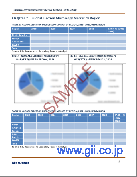
地域別の概況
電子顕微鏡市場は、北米、欧州、アジア太平洋、LAMEAの各地域で分析されています。アジア太平洋地域は、2021年に電子顕微鏡市場で有望な収益シェアを獲得しました。アジア太平洋地域は、顕微鏡研究のための研究開発資金の増加、ライフサイエンスやナノテクノロジー研究における相関顕微鏡の使用拡大、顕微鏡研究のためのコラボレーションセンターの設立、OEMのための原材料や熟練労働者の手頃な価格などの要因によって燃料を供給されています。
市場参加者がとる主な戦略は、製品の上市です。カーディナルマトリックスで提示された分析に基づき、サーモフィッシャーサイエンティフィック社は電子顕微鏡市場の先駆者です。Advantest Corporation、Carl Zeiss AG、Bruker Corporationなどの企業は、電子顕微鏡市場の主要な革新者の一部です。
目次
第1章 市場の範囲と調査手法
- 市場の定義.
- 目的.
- 市場規模.
- セグメンテーション.
- 電子顕微鏡の世界市場、タイプ別
- 電子顕微鏡の世界市場、アプリケーション別
- 電子顕微鏡の世界市場、エンドユーザー別
- 電子顕微鏡の世界市場、地域別
- 調査手法
第2章 市場概要
- イントロダクション.
- 概要の説明
- 市場の構成とシナリオ.
- 概要の説明
- 市場に影響を与える主要因.
- 市場促進要因.
- 市場の抑制要因.
第3章 競合分析-世界
- KBVカーディナルマトリックス
- 最近の業界全体の戦略的展開
- パートナーシップ、コラボレーション、契約
- 製品上市と製品拡張
- 買収と合併
- トップ・ウィニング・ストラテジー
- 主要なリーディング戦略:パーセンテージ分布(2018-2022)
- 主要な戦略的動き:(製品発表と製品拡張:2018年、8月~2022年、6月)主要なプレーヤーたち
第4章 電子顕微鏡の世界市場:タイプ別
- スキャニングの世界市場:地域別
- トランスミッションの世界市場:地域別
第5章 電子顕微鏡の世界市場:アプリケーション別
- 半導体の世界市場:地域別
- ライフサイエンスの世界市場:地域別
- マテリアルサイエンス&その他の世界市場:地域別
第6章 電子顕微鏡の世界市場:エンドユーザー別
- 産業界の世界市場:地域別
- 学術・研究機関の世界市場:地域別
- その他分野の世界市場:地域別
第7章 電子顕微鏡の世界市場:地域別
- 北米.
- 北米の電子顕微鏡の国別市場
- 米国
- カナダ
- メキシコ
- 北米以外の地域
- 北米の電子顕微鏡の国別市場
- 欧州
- 欧州電子顕微鏡市場:国別
- ドイツ
- 英国
- フランス
- ロシア
- スペイン
- イタリア
- その他欧州
- 欧州電子顕微鏡市場:国別
- アジア太平洋地域
- アジア太平洋地域の電子顕微鏡市場:国別内訳
- 中国
- 日本
- インド
- 韓国
- シンガポール
- マレーシア
- その他アジア太平洋地域
- アジア太平洋地域の電子顕微鏡市場:国別内訳
- LAMEA
- LAMEA電子顕微鏡の国別市場
- ブラジル
- アルゼンチン
- UAE
- サウジアラビア
- 南アフリカ共和国
- ナイジェリア
- LAMEAの他の地域
- LAMEA電子顕微鏡の国別市場
第8章 企業プロファイル
- Thermo Fisher Scientific, Inc.
- Bruker Corporation
- Carl Zeiss AG
- Advantest Corporation
- Nikon Instruments, Inc.(Nikon Healthcare)(Nikon Corporation)
- Hitachi High-Tech Corporation(Hitachi, Ltd.)
- JEOL, Ltd.
- Oxford Instruments plc
- TESCAN ORSAY HOLDING, a.s.
- DELONG INSTRUMENTS a. s.
LIST OF TABLES
- TABLE 1 Global Electron Microscopy Market, 2018 - 2021, USD Million
- TABLE 2 Global Electron Microscopy Market, 2022 - 2028, USD Million
- TABLE 3 Partnerships, Collaborations and Agreements- Electron Microscopy Market
- TABLE 4 Product Launches And Product Expansions- Electron Microscopy Market
- TABLE 5 Acquisition and Mergers- Electron Microscopy Market
- TABLE 6 Global Electron Microscopy Market by Type, 2018 - 2021, USD Million
- TABLE 7 Global Electron Microscopy Market by Type, 2022 - 2028, USD Million
- TABLE 8 Global Scanning Market by Region, 2018 - 2021, USD Million
- TABLE 9 Global Scanning Market by Region, 2022 - 2028, USD Million
- TABLE 10 Global Transmission Market by Region, 2018 - 2021, USD Million
- TABLE 11 Global Transmission Market by Region, 2022 - 2028, USD Million
- TABLE 12 Global Electron Microscopy Market by Application, 2018 - 2021, USD Million
- TABLE 13 Global Electron Microscopy Market by Application, 2022 - 2028, USD Million
- TABLE 14 Global Semiconductors Market by Region, 2018 - 2021, USD Million
- TABLE 15 Global Semiconductors Market by Region, 2022 - 2028, USD Million
- TABLE 16 Global Life Sciences Market by Region, 2018 - 2021, USD Million
- TABLE 17 Global Life Sciences Market by Region, 2022 - 2028, USD Million
- TABLE 18 Global Material Sciences & Others Market by Region, 2018 - 2021, USD Million
- TABLE 19 Global Material Sciences & Others Market by Region, 2022 - 2028, USD Million
- TABLE 20 Global Electron Microscopy Market by End User, 2018 - 2021, USD Million
- TABLE 21 Global Electron Microscopy Market by End User, 2022 - 2028, USD Million
- TABLE 22 Global Industries Market by Region, 2018 - 2021, USD Million
- TABLE 23 Global Industries Market by Region, 2022 - 2028, USD Million
- TABLE 24 Global Academic & Research Institutes Market by Region, 2018 - 2021, USD Million
- TABLE 25 Global Academic & Research Institutes Market by Region, 2022 - 2028, USD Million
- TABLE 26 Global Others Market by Region, 2018 - 2021, USD Million
- TABLE 27 Global Others Market by Region, 2022 - 2028, USD Million
- TABLE 28 Global Electron Microscopy Market by Region, 2018 - 2021, USD Million
- TABLE 29 Global Electron Microscopy Market by Region, 2022 - 2028, USD Million
- TABLE 30 North America Electron Microscopy Market, 2018 - 2021, USD Million
- TABLE 31 North America Electron Microscopy Market, 2022 - 2028, USD Million
- TABLE 32 North America Electron Microscopy Market by Type, 2018 - 2021, USD Million
- TABLE 33 North America Electron Microscopy Market by Type, 2022 - 2028, USD Million
- TABLE 34 North America Scanning Market by Country, 2018 - 2021, USD Million
- TABLE 35 North America Scanning Market by Country, 2022 - 2028, USD Million
- TABLE 36 North America Transmission Market by Country, 2018 - 2021, USD Million
- TABLE 37 North America Transmission Market by Country, 2022 - 2028, USD Million
- TABLE 38 North America Electron Microscopy Market by Application, 2018 - 2021, USD Million
- TABLE 39 North America Electron Microscopy Market by Application, 2022 - 2028, USD Million
- TABLE 40 North America Semiconductors Market by Country, 2018 - 2021, USD Million
- TABLE 41 North America Semiconductors Market by Country, 2022 - 2028, USD Million
- TABLE 42 North America Life Sciences Market by Country, 2018 - 2021, USD Million
- TABLE 43 North America Life Sciences Market by Country, 2022 - 2028, USD Million
- TABLE 44 North America Material Sciences & Others Market by Country, 2018 - 2021, USD Million
- TABLE 45 North America Material Sciences & Others Market by Country, 2022 - 2028, USD Million
- TABLE 46 North America Electron Microscopy Market by End User, 2018 - 2021, USD Million
- TABLE 47 North America Electron Microscopy Market by End User, 2022 - 2028, USD Million
- TABLE 48 North America Industries Market by Country, 2018 - 2021, USD Million
- TABLE 49 North America Industries Market by Country, 2022 - 2028, USD Million
- TABLE 50 North America Academic & Research Institutes Market by Country, 2018 - 2021, USD Million
- TABLE 51 North America Academic & Research Institutes Market by Country, 2022 - 2028, USD Million
- TABLE 52 North America Others Market by Country, 2018 - 2021, USD Million
- TABLE 53 North America Others Market by Country, 2022 - 2028, USD Million
- TABLE 54 North America Electron Microscopy Market by Country, 2018 - 2021, USD Million
- TABLE 55 North America Electron Microscopy Market by Country, 2022 - 2028, USD Million
- TABLE 56 US Electron Microscopy Market, 2018 - 2021, USD Million
- TABLE 57 US Electron Microscopy Market, 2022 - 2028, USD Million
- TABLE 58 US Electron Microscopy Market by Type, 2018 - 2021, USD Million
- TABLE 59 US Electron Microscopy Market by Type, 2022 - 2028, USD Million
- TABLE 60 US Electron Microscopy Market by Application, 2018 - 2021, USD Million
- TABLE 61 US Electron Microscopy Market by Application, 2022 - 2028, USD Million
- TABLE 62 US Electron Microscopy Market by End User, 2018 - 2021, USD Million
- TABLE 63 US Electron Microscopy Market by End User, 2022 - 2028, USD Million
- TABLE 64 Canada Electron Microscopy Market, 2018 - 2021, USD Million
- TABLE 65 Canada Electron Microscopy Market, 2022 - 2028, USD Million
- TABLE 66 Canada Electron Microscopy Market by Type, 2018 - 2021, USD Million
- TABLE 67 Canada Electron Microscopy Market by Type, 2022 - 2028, USD Million
- TABLE 68 Canada Electron Microscopy Market by Application, 2018 - 2021, USD Million
- TABLE 69 Canada Electron Microscopy Market by Application, 2022 - 2028, USD Million
- TABLE 70 Canada Electron Microscopy Market by End User, 2018 - 2021, USD Million
- TABLE 71 Canada Electron Microscopy Market by End User, 2022 - 2028, USD Million
- TABLE 72 Mexico Electron Microscopy Market, 2018 - 2021, USD Million
- TABLE 73 Mexico Electron Microscopy Market, 2022 - 2028, USD Million
- TABLE 74 Mexico Electron Microscopy Market by Type, 2018 - 2021, USD Million
- TABLE 75 Mexico Electron Microscopy Market by Type, 2022 - 2028, USD Million
- TABLE 76 Mexico Electron Microscopy Market by Application, 2018 - 2021, USD Million
- TABLE 77 Mexico Electron Microscopy Market by Application, 2022 - 2028, USD Million
- TABLE 78 Mexico Electron Microscopy Market by End User, 2018 - 2021, USD Million
- TABLE 79 Mexico Electron Microscopy Market by End User, 2022 - 2028, USD Million
- TABLE 80 Rest of North America Electron Microscopy Market, 2018 - 2021, USD Million
- TABLE 81 Rest of North America Electron Microscopy Market, 2022 - 2028, USD Million
- TABLE 82 Rest of North America Electron Microscopy Market by Type, 2018 - 2021, USD Million
- TABLE 83 Rest of North America Electron Microscopy Market by Type, 2022 - 2028, USD Million
- TABLE 84 Rest of North America Electron Microscopy Market by Application, 2018 - 2021, USD Million
- TABLE 85 Rest of North America Electron Microscopy Market by Application, 2022 - 2028, USD Million
- TABLE 86 Rest of North America Electron Microscopy Market by End User, 2018 - 2021, USD Million
- TABLE 87 Rest of North America Electron Microscopy Market by End User, 2022 - 2028, USD Million
- TABLE 88 Europe Electron Microscopy Market, 2018 - 2021, USD Million
- TABLE 89 Europe Electron Microscopy Market, 2022 - 2028, USD Million
- TABLE 90 Europe Electron Microscopy Market by Type, 2018 - 2021, USD Million
- TABLE 91 Europe Electron Microscopy Market by Type, 2022 - 2028, USD Million
- TABLE 92 Europe Scanning Market by Country, 2018 - 2021, USD Million
- TABLE 93 Europe Scanning Market by Country, 2022 - 2028, USD Million
- TABLE 94 Europe Transmission Market by Country, 2018 - 2021, USD Million
- TABLE 95 Europe Transmission Market by Country, 2022 - 2028, USD Million
- TABLE 96 Europe Electron Microscopy Market by Application, 2018 - 2021, USD Million
- TABLE 97 Europe Electron Microscopy Market by Application, 2022 - 2028, USD Million
- TABLE 98 Europe Semiconductors Market by Country, 2018 - 2021, USD Million
- TABLE 99 Europe Semiconductors Market by Country, 2022 - 2028, USD Million
- TABLE 100 Europe Life Sciences Market by Country, 2018 - 2021, USD Million
- TABLE 101 Europe Life Sciences Market by Country, 2022 - 2028, USD Million
- TABLE 102 Europe Material Sciences & Others Market by Country, 2018 - 2021, USD Million
- TABLE 103 Europe Material Sciences & Others Market by Country, 2022 - 2028, USD Million
- TABLE 104 Europe Electron Microscopy Market by End User, 2018 - 2021, USD Million
- TABLE 105 Europe Electron Microscopy Market by End User, 2022 - 2028, USD Million
- TABLE 106 Europe Industries Market by Country, 2018 - 2021, USD Million
- TABLE 107 Europe Industries Market by Country, 2022 - 2028, USD Million
- TABLE 108 Europe Academic & Research Institutes Market by Country, 2018 - 2021, USD Million
- TABLE 109 Europe Academic & Research Institutes Market by Country, 2022 - 2028, USD Million
- TABLE 110 Europe Others Market by Country, 2018 - 2021, USD Million
- TABLE 111 Europe Others Market by Country, 2022 - 2028, USD Million
- TABLE 112 Europe Electron Microscopy Market by Country, 2018 - 2021, USD Million
- TABLE 113 Europe Electron Microscopy Market by Country, 2022 - 2028, USD Million
- TABLE 114 Germany Electron Microscopy Market, 2018 - 2021, USD Million
- TABLE 115 Germany Electron Microscopy Market, 2022 - 2028, USD Million
- TABLE 116 Germany Electron Microscopy Market by Type, 2018 - 2021, USD Million
- TABLE 117 Germany Electron Microscopy Market by Type, 2022 - 2028, USD Million
- TABLE 118 Germany Electron Microscopy Market by Application, 2018 - 2021, USD Million
- TABLE 119 Germany Electron Microscopy Market by Application, 2022 - 2028, USD Million
- TABLE 120 Germany Electron Microscopy Market by End User, 2018 - 2021, USD Million
- TABLE 121 Germany Electron Microscopy Market by End User, 2022 - 2028, USD Million
- TABLE 122 UK Electron Microscopy Market, 2018 - 2021, USD Million
- TABLE 123 UK Electron Microscopy Market, 2022 - 2028, USD Million
- TABLE 124 UK Electron Microscopy Market by Type, 2018 - 2021, USD Million
- TABLE 125 UK Electron Microscopy Market by Type, 2022 - 2028, USD Million
- TABLE 126 UK Electron Microscopy Market by Application, 2018 - 2021, USD Million
- TABLE 127 UK Electron Microscopy Market by Application, 2022 - 2028, USD Million
- TABLE 128 UK Electron Microscopy Market by End User, 2018 - 2021, USD Million
- TABLE 129 UK Electron Microscopy Market by End User, 2022 - 2028, USD Million
- TABLE 130 France Electron Microscopy Market, 2018 - 2021, USD Million
- TABLE 131 France Electron Microscopy Market, 2022 - 2028, USD Million
- TABLE 132 France Electron Microscopy Market by Type, 2018 - 2021, USD Million
- TABLE 133 France Electron Microscopy Market by Type, 2022 - 2028, USD Million
- TABLE 134 France Electron Microscopy Market by Application, 2018 - 2021, USD Million
- TABLE 135 France Electron Microscopy Market by Application, 2022 - 2028, USD Million
- TABLE 136 France Electron Microscopy Market by End User, 2018 - 2021, USD Million
- TABLE 137 France Electron Microscopy Market by End User, 2022 - 2028, USD Million
- TABLE 138 Russia Electron Microscopy Market, 2018 - 2021, USD Million
- TABLE 139 Russia Electron Microscopy Market, 2022 - 2028, USD Million
- TABLE 140 Russia Electron Microscopy Market by Type, 2018 - 2021, USD Million
- TABLE 141 Russia Electron Microscopy Market by Type, 2022 - 2028, USD Million
- TABLE 142 Russia Electron Microscopy Market by Application, 2018 - 2021, USD Million
- TABLE 143 Russia Electron Microscopy Market by Application, 2022 - 2028, USD Million
- TABLE 144 Russia Electron Microscopy Market by End User, 2018 - 2021, USD Million
- TABLE 145 Russia Electron Microscopy Market by End User, 2022 - 2028, USD Million
- TABLE 146 Spain Electron Microscopy Market, 2018 - 2021, USD Million
- TABLE 147 Spain Electron Microscopy Market, 2022 - 2028, USD Million
- TABLE 148 Spain Electron Microscopy Market by Type, 2018 - 2021, USD Million
- TABLE 149 Spain Electron Microscopy Market by Type, 2022 - 2028, USD Million
- TABLE 150 Spain Electron Microscopy Market by Application, 2018 - 2021, USD Million
- TABLE 151 Spain Electron Microscopy Market by Application, 2022 - 2028, USD Million
- TABLE 152 Spain Electron Microscopy Market by End User, 2018 - 2021, USD Million
- TABLE 153 Spain Electron Microscopy Market by End User, 2022 - 2028, USD Million
- TABLE 154 Italy Electron Microscopy Market, 2018 - 2021, USD Million
- TABLE 155 Italy Electron Microscopy Market, 2022 - 2028, USD Million
- TABLE 156 Italy Electron Microscopy Market by Type, 2018 - 2021, USD Million
- TABLE 157 Italy Electron Microscopy Market by Type, 2022 - 2028, USD Million
- TABLE 158 Italy Electron Microscopy Market by Application, 2018 - 2021, USD Million
- TABLE 159 Italy Electron Microscopy Market by Application, 2022 - 2028, USD Million
- TABLE 160 Italy Electron Microscopy Market by End User, 2018 - 2021, USD Million
- TABLE 161 Italy Electron Microscopy Market by End User, 2022 - 2028, USD Million
- TABLE 162 Rest of Europe Electron Microscopy Market, 2018 - 2021, USD Million
- TABLE 163 Rest of Europe Electron Microscopy Market, 2022 - 2028, USD Million
- TABLE 164 Rest of Europe Electron Microscopy Market by Type, 2018 - 2021, USD Million
- TABLE 165 Rest of Europe Electron Microscopy Market by Type, 2022 - 2028, USD Million
- TABLE 166 Rest of Europe Electron Microscopy Market by Application, 2018 - 2021, USD Million
- TABLE 167 Rest of Europe Electron Microscopy Market by Application, 2022 - 2028, USD Million
- TABLE 168 Rest of Europe Electron Microscopy Market by End User, 2018 - 2021, USD Million
- TABLE 169 Rest of Europe Electron Microscopy Market by End User, 2022 - 2028, USD Million
- TABLE 170 Asia Pacific Electron Microscopy Market, 2018 - 2021, USD Million
- TABLE 171 Asia Pacific Electron Microscopy Market, 2022 - 2028, USD Million
- TABLE 172 Asia Pacific Electron Microscopy Market by Type, 2018 - 2021, USD Million
- TABLE 173 Asia Pacific Electron Microscopy Market by Type, 2022 - 2028, USD Million
- TABLE 174 Asia Pacific Scanning Market by Country, 2018 - 2021, USD Million
- TABLE 175 Asia Pacific Scanning Market by Country, 2022 - 2028, USD Million
- TABLE 176 Asia Pacific Transmission Market by Country, 2018 - 2021, USD Million
- TABLE 177 Asia Pacific Transmission Market by Country, 2022 - 2028, USD Million
- TABLE 178 Asia Pacific Electron Microscopy Market by Application, 2018 - 2021, USD Million
- TABLE 179 Asia Pacific Electron Microscopy Market by Application, 2022 - 2028, USD Million
- TABLE 180 Asia Pacific Semiconductors Market by Country, 2018 - 2021, USD Million
- TABLE 181 Asia Pacific Semiconductors Market by Country, 2022 - 2028, USD Million
- TABLE 182 Asia Pacific Life Sciences Market by Country, 2018 - 2021, USD Million
- TABLE 183 Asia Pacific Life Sciences Market by Country, 2022 - 2028, USD Million
- TABLE 184 Asia Pacific Material Sciences & Others Market by Country, 2018 - 2021, USD Million
- TABLE 185 Asia Pacific Material Sciences & Others Market by Country, 2022 - 2028, USD Million
- TABLE 186 Asia Pacific Electron Microscopy Market by End User, 2018 - 2021, USD Million
- TABLE 187 Asia Pacific Electron Microscopy Market by End User, 2022 - 2028, USD Million
- TABLE 188 Asia Pacific Industries Market by Country, 2018 - 2021, USD Million
- TABLE 189 Asia Pacific Industries Market by Country, 2022 - 2028, USD Million
- TABLE 190 Asia Pacific Academic & Research Institutes Market by Country, 2018 - 2021, USD Million
- TABLE 191 Asia Pacific Academic & Research Institutes Market by Country, 2022 - 2028, USD Million
- TABLE 192 Asia Pacific Others Market by Country, 2018 - 2021, USD Million
- TABLE 193 Asia Pacific Others Market by Country, 2022 - 2028, USD Million
- TABLE 194 Asia Pacific Electron Microscopy Market by Country, 2018 - 2021, USD Million
- TABLE 195 Asia Pacific Electron Microscopy Market by Country, 2022 - 2028, USD Million
- TABLE 196 China Electron Microscopy Market, 2018 - 2021, USD Million
- TABLE 197 China Electron Microscopy Market, 2022 - 2028, USD Million
- TABLE 198 China Electron Microscopy Market by Type, 2018 - 2021, USD Million
- TABLE 199 China Electron Microscopy Market by Type, 2022 - 2028, USD Million
- TABLE 200 China Electron Microscopy Market by Application, 2018 - 2021, USD Million
- TABLE 201 China Electron Microscopy Market by Application, 2022 - 2028, USD Million
- TABLE 202 China Electron Microscopy Market by End User, 2018 - 2021, USD Million
- TABLE 203 China Electron Microscopy Market by End User, 2022 - 2028, USD Million
- TABLE 204 Japan Electron Microscopy Market, 2018 - 2021, USD Million
- TABLE 205 Japan Electron Microscopy Market, 2022 - 2028, USD Million
- TABLE 206 Japan Electron Microscopy Market by Type, 2018 - 2021, USD Million
- TABLE 207 Japan Electron Microscopy Market by Type, 2022 - 2028, USD Million
- TABLE 208 Japan Electron Microscopy Market by Application, 2018 - 2021, USD Million
- TABLE 209 Japan Electron Microscopy Market by Application, 2022 - 2028, USD Million
- TABLE 210 Japan Electron Microscopy Market by End User, 2018 - 2021, USD Million
- TABLE 211 Japan Electron Microscopy Market by End User, 2022 - 2028, USD Million
- TABLE 212 India Electron Microscopy Market, 2018 - 2021, USD Million
- TABLE 213 India Electron Microscopy Market, 2022 - 2028, USD Million
- TABLE 214 India Electron Microscopy Market by Type, 2018 - 2021, USD Million
- TABLE 215 India Electron Microscopy Market by Type, 2022 - 2028, USD Million
- TABLE 216 India Electron Microscopy Market by Application, 2018 - 2021, USD Million
- TABLE 217 India Electron Microscopy Market by Application, 2022 - 2028, USD Million
- TABLE 218 India Electron Microscopy Market by End User, 2018 - 2021, USD Million
- TABLE 219 India Electron Microscopy Market by End User, 2022 - 2028, USD Million
- TABLE 220 South Korea Electron Microscopy Market, 2018 - 2021, USD Million
- TABLE 221 South Korea Electron Microscopy Market, 2022 - 2028, USD Million
- TABLE 222 South Korea Electron Microscopy Market by Type, 2018 - 2021, USD Million
- TABLE 223 South Korea Electron Microscopy Market by Type, 2022 - 2028, USD Million
- TABLE 224 South Korea Electron Microscopy Market by Application, 2018 - 2021, USD Million
- TABLE 225 South Korea Electron Microscopy Market by Application, 2022 - 2028, USD Million
- TABLE 226 South Korea Electron Microscopy Market by End User, 2018 - 2021, USD Million
- TABLE 227 South Korea Electron Microscopy Market by End User, 2022 - 2028, USD Million
- TABLE 228 Singapore Electron Microscopy Market, 2018 - 2021, USD Million
- TABLE 229 Singapore Electron Microscopy Market, 2022 - 2028, USD Million
- TABLE 230 Singapore Electron Microscopy Market by Type, 2018 - 2021, USD Million
- TABLE 231 Singapore Electron Microscopy Market by Type, 2022 - 2028, USD Million
- TABLE 232 Singapore Electron Microscopy Market by Application, 2018 - 2021, USD Million
- TABLE 233 Singapore Electron Microscopy Market by Application, 2022 - 2028, USD Million
- TABLE 234 Singapore Electron Microscopy Market by End User, 2018 - 2021, USD Million
- TABLE 235 Singapore Electron Microscopy Market by End User, 2022 - 2028, USD Million
- TABLE 236 Malaysia Electron Microscopy Market, 2018 - 2021, USD Million
- TABLE 237 Malaysia Electron Microscopy Market, 2022 - 2028, USD Million
- TABLE 238 Malaysia Electron Microscopy Market by Type, 2018 - 2021, USD Million
- TABLE 239 Malaysia Electron Microscopy Market by Type, 2022 - 2028, USD Million
- TABLE 240 Malaysia Electron Microscopy Market by Application, 2018 - 2021, USD Million
- TABLE 241 Malaysia Electron Microscopy Market by Application, 2022 - 2028, USD Million
- TABLE 242 Malaysia Electron Microscopy Market by End User, 2018 - 2021, USD Million
- TABLE 243 Malaysia Electron Microscopy Market by End User, 2022 - 2028, USD Million
- TABLE 244 Rest of Asia Pacific Electron Microscopy Market, 2018 - 2021, USD Million
- TABLE 245 Rest of Asia Pacific Electron Microscopy Market, 2022 - 2028, USD Million
- TABLE 246 Rest of Asia Pacific Electron Microscopy Market by Type, 2018 - 2021, USD Million
- TABLE 247 Rest of Asia Pacific Electron Microscopy Market by Type, 2022 - 2028, USD Million
- TABLE 248 Rest of Asia Pacific Electron Microscopy Market by Application, 2018 - 2021, USD Million
- TABLE 249 Rest of Asia Pacific Electron Microscopy Market by Application, 2022 - 2028, USD Million
- TABLE 250 Rest of Asia Pacific Electron Microscopy Market by End User, 2018 - 2021, USD Million
- TABLE 251 Rest of Asia Pacific Electron Microscopy Market by End User, 2022 - 2028, USD Million
- TABLE 252 LAMEA Electron Microscopy Market, 2018 - 2021, USD Million
- TABLE 253 LAMEA Electron Microscopy Market, 2022 - 2028, USD Million
- TABLE 254 LAMEA Electron Microscopy Market by Type, 2018 - 2021, USD Million
- TABLE 255 LAMEA Electron Microscopy Market by Type, 2022 - 2028, USD Million
- TABLE 256 LAMEA Scanning Market by Country, 2018 - 2021, USD Million
- TABLE 257 LAMEA Scanning Market by Country, 2022 - 2028, USD Million
- TABLE 258 LAMEA Transmission Market by Country, 2018 - 2021, USD Million
- TABLE 259 LAMEA Transmission Market by Country, 2022 - 2028, USD Million
- TABLE 260 LAMEA Electron Microscopy Market by Application, 2018 - 2021, USD Million
- TABLE 261 LAMEA Electron Microscopy Market by Application, 2022 - 2028, USD Million
- TABLE 262 LAMEA Semiconductors Market by Country, 2018 - 2021, USD Million
- TABLE 263 LAMEA Semiconductors Market by Country, 2022 - 2028, USD Million
- TABLE 264 LAMEA Life Sciences Market by Country, 2018 - 2021, USD Million
- TABLE 265 LAMEA Life Sciences Market by Country, 2022 - 2028, USD Million
- TABLE 266 LAMEA Material Sciences & Others Market by Country, 2018 - 2021, USD Million
- TABLE 267 LAMEA Material Sciences & Others Market by Country, 2022 - 2028, USD Million
- TABLE 268 LAMEA Electron Microscopy Market by End User, 2018 - 2021, USD Million
- TABLE 269 LAMEA Electron Microscopy Market by End User, 2022 - 2028, USD Million
- TABLE 270 LAMEA Industries Market by Country, 2018 - 2021, USD Million
- TABLE 271 LAMEA Industries Market by Country, 2022 - 2028, USD Million
- TABLE 272 LAMEA Academic & Research Institutes Market by Country, 2018 - 2021, USD Million
- TABLE 273 LAMEA Academic & Research Institutes Market by Country, 2022 - 2028, USD Million
- TABLE 274 LAMEA Others Market by Country, 2018 - 2021, USD Million
- TABLE 275 LAMEA Others Market by Country, 2022 - 2028, USD Million
- TABLE 276 LAMEA Electron Microscopy Market by Country, 2018 - 2021, USD Million
- TABLE 277 LAMEA Electron Microscopy Market by Country, 2022 - 2028, USD Million
- TABLE 278 Brazil Electron Microscopy Market, 2018 - 2021, USD Million
- TABLE 279 Brazil Electron Microscopy Market, 2022 - 2028, USD Million
- TABLE 280 Brazil Electron Microscopy Market by Type, 2018 - 2021, USD Million
- TABLE 281 Brazil Electron Microscopy Market by Type, 2022 - 2028, USD Million
- TABLE 282 Brazil Electron Microscopy Market by Application, 2018 - 2021, USD Million
- TABLE 283 Brazil Electron Microscopy Market by Application, 2022 - 2028, USD Million
- TABLE 284 Brazil Electron Microscopy Market by End User, 2018 - 2021, USD Million
- TABLE 285 Brazil Electron Microscopy Market by End User, 2022 - 2028, USD Million
- TABLE 286 Argentina Electron Microscopy Market, 2018 - 2021, USD Million
- TABLE 287 Argentina Electron Microscopy Market, 2022 - 2028, USD Million
- TABLE 288 Argentina Electron Microscopy Market by Type, 2018 - 2021, USD Million
- TABLE 289 Argentina Electron Microscopy Market by Type, 2022 - 2028, USD Million
- TABLE 290 Argentina Electron Microscopy Market by Application, 2018 - 2021, USD Million
- TABLE 291 Argentina Electron Microscopy Market by Application, 2022 - 2028, USD Million
- TABLE 292 Argentina Electron Microscopy Market by End User, 2018 - 2021, USD Million
- TABLE 293 Argentina Electron Microscopy Market by End User, 2022 - 2028, USD Million
- TABLE 294 UAE Electron Microscopy Market, 2018 - 2021, USD Million
- TABLE 295 UAE Electron Microscopy Market, 2022 - 2028, USD Million
- TABLE 296 UAE Electron Microscopy Market by Type, 2018 - 2021, USD Million
- TABLE 297 UAE Electron Microscopy Market by Type, 2022 - 2028, USD Million
- TABLE 298 UAE Electron Microscopy Market by Application, 2018 - 2021, USD Million
- TABLE 299 UAE Electron Microscopy Market by Application, 2022 - 2028, USD Million
- TABLE 300 UAE Electron Microscopy Market by End User, 2018 - 2021, USD Million
- TABLE 301 UAE Electron Microscopy Market by End User, 2022 - 2028, USD Million
- TABLE 302 Saudi Arabia Electron Microscopy Market, 2018 - 2021, USD Million
- TABLE 303 Saudi Arabia Electron Microscopy Market, 2022 - 2028, USD Million
- TABLE 304 Saudi Arabia Electron Microscopy Market by Type, 2018 - 2021, USD Million
- TABLE 305 Saudi Arabia Electron Microscopy Market by Type, 2022 - 2028, USD Million
- TABLE 306 Saudi Arabia Electron Microscopy Market by Application, 2018 - 2021, USD Million
- TABLE 307 Saudi Arabia Electron Microscopy Market by Application, 2022 - 2028, USD Million
- TABLE 308 Saudi Arabia Electron Microscopy Market by End User, 2018 - 2021, USD Million
- TABLE 309 Saudi Arabia Electron Microscopy Market by End User, 2022 - 2028, USD Million
- TABLE 310 South Africa Electron Microscopy Market, 2018 - 2021, USD Million
- TABLE 311 South Africa Electron Microscopy Market, 2022 - 2028, USD Million
- TABLE 312 South Africa Electron Microscopy Market by Type, 2018 - 2021, USD Million
- TABLE 313 South Africa Electron Microscopy Market by Type, 2022 - 2028, USD Million
- TABLE 314 South Africa Electron Microscopy Market by Application, 2018 - 2021, USD Million
- TABLE 315 South Africa Electron Microscopy Market by Application, 2022 - 2028, USD Million
- TABLE 316 South Africa Electron Microscopy Market by End User, 2018 - 2021, USD Million
- TABLE 317 South Africa Electron Microscopy Market by End User, 2022 - 2028, USD Million
- TABLE 318 Nigeria Electron Microscopy Market, 2018 - 2021, USD Million
- TABLE 319 Nigeria Electron Microscopy Market, 2022 - 2028, USD Million
- TABLE 320 Nigeria Electron Microscopy Market by Type, 2018 - 2021, USD Million
- TABLE 321 Nigeria Electron Microscopy Market by Type, 2022 - 2028, USD Million
- TABLE 322 Nigeria Electron Microscopy Market by Application, 2018 - 2021, USD Million
- TABLE 323 Nigeria Electron Microscopy Market by Application, 2022 - 2028, USD Million
- TABLE 324 Nigeria Electron Microscopy Market by End User, 2018 - 2021, USD Million
- TABLE 325 Nigeria Electron Microscopy Market by End User, 2022 - 2028, USD Million
- TABLE 326 Rest of LAMEA Electron Microscopy Market, 2018 - 2021, USD Million
- TABLE 327 Rest of LAMEA Electron Microscopy Market, 2022 - 2028, USD Million
- TABLE 328 Rest of LAMEA Electron Microscopy Market by Type, 2018 - 2021, USD Million
- TABLE 329 Rest of LAMEA Electron Microscopy Market by Type, 2022 - 2028, USD Million
- TABLE 330 Rest of LAMEA Electron Microscopy Market by Application, 2018 - 2021, USD Million
- TABLE 331 Rest of LAMEA Electron Microscopy Market by Application, 2022 - 2028, USD Million
- TABLE 332 Rest of LAMEA Electron Microscopy Market by End User, 2018 - 2021, USD Million
- TABLE 333 Rest of LAMEA Electron Microscopy Market by End User, 2022 - 2028, USD Million
- TABLE 334 Key Information - Thermo Fisher Scientific, Inc.
- TABLE 335 Key Information - Bruker Corporation
- TABLE 336 Key Information - Carl Zeiss AG
- TABLE 337 Key Information - Advantest Corporation
- TABLE 338 Key Information - Nikon Instruments, Inc.
- TABLE 339 Key Information - Hitachi High-Tech Corporation
- TABLE 340 Key Information - JEOL, Ltd.
- TABLE 341 Key Information - Oxford Instruments plc
- TABLE 342 Key Information - TESCAN ORSAY HOLDING, a.s.
- TABLE 343 Key Information - DELONG INSTRUMENTS a. s.
List of Figures
- FIG 1 Methodology for the research
- FIG 2 KBV Cardinal Matrix
- FIG 3 Key Leading Strategies: Percentage Distribution (2018-2022)
- FIG 4 Key Strategic Move: (Product Launches and Product Expansions : 2018, Aug - 2022, Jun) Leading Players
- FIG 5 Global Electron Microscopy Market share by Type, 2021
- FIG 6 Global Electron Microscopy Market share by Type, 2028
- FIG 7 Global Electron Microscopy Market by Type, 2018 - 2028, USD Million
- FIG 8 Global Electron Microscopy Market share by Application, 2021
- FIG 9 Global Electron Microscopy Market share by Application, 2028
- FIG 10 Global Electron Microscopy Market by Application, 2018 - 2028, USD Million
- FIG 11 Global Electron Microscopy Market share by End User, 2021
- FIG 12 Global Electron Microscopy Market share by End User, 2028
- FIG 13 Global Electron Microscopy Market by End User, 2018 - 2028, USD Million
- FIG 14 Global Electron Microscopy Market share by Region, 2021
- FIG 15 Global Electron Microscopy Market share by Region, 2028
- FIG 16 Global Electron Microscopy Market by Region, 2018 - 2028, USD Million
- FIG 17 Swot analysis: Thermo Fisher Scientific, Inc.
- FIG 18 Recent strategies and developments: Bruker Corporation
- FIG 19 Recent strategies and developments: Carl Zeiss AG
- FIG 20 Recent strategies and developments: Advantest Corporation
- FIG 21 Recent strategies and developments: Oxford Instruments plc
- FIG 22 Recent strategies and developments: TESCAN ORSAY HOLDING, a.s.
The Global Electron Microscopy Market size is expected to reach $5.2 billion by 2028, rising at a market growth of 7.8% CAGR during the forecast period.
Electron microscopy (EM) is a technique for taking high-resolution pictures of both biological and non-biological material. It is employed in biomedical research to look at the precise structure of organelles, macromolecular complexes, tissues, cells, and cells. The utilization of electrons as the source of illuminating radiation, which has extremely short wavelengths, contributes to the great resolution of EM pictures. To address particular issues, electron microscopy is combined with a range of auxiliary methods (such as thin sectioning, immuno-labeling, and negative staining.
For traditional scanning electron microscopy to work, secondary electrons must be emitted from a specimen's surface. A scanning electron microscope is the equivalent of a stereo light microscope in the EM because of its superior depth of focus. It offers intricate pictures of the surfaces of cells and entire organisms, which TEM cannot do. Additionally, it can be utilized for process control, particle size analysis, and counting. Because the image is created by rastering a focused electron beam across the specimen's surface, it is known as a scanning electron microscope.
Each point in the raster emits particles as a result of the primary electron beam's interaction with atoms close to the surface low energy secondary electrons, high-energy backscatter electrons, X-rays, and even photons. These can be gathered using a variety of detectors, and the brightness at each analogous position on a cathode ray tube can be calculated from their relative number. The final image is an enlarged image of the specimen since the size of the raster at the specimen is significantly smaller than the viewing screen of the CRT. SEMs that are properly set up (with secondary, backscatter, and X-ray detectors) can be used to examine specimen topography, atomic composition, as well as, the distribution of immuno-labels on the specimen's surface.
COVID-19 Impact Analysis
Trade and economic activity have been impacted by the COVID-19 outbreak everywhere in the world. While the small software industry for the automotive and aerospace industries is expected to suffer, the tiny software market for the healthcare and semiconductor industries is expected to grow. Production and manufacturing have been significantly impacted as a result of several countries around the world declaring statewide lockdowns and temporary closures of various industries. Trade restrictions have made the demand-supply mismatch worse. The COVID-19 pandemic will affect companies that make semiconductors for the electron microscope market in a variety of ways, both now and in the future.
Market Growth Factors
Improvements In Microscopy Technology
Digitization, super-resolution, live-cell imaging, and high throughput techniques are examples of technological developments in microscopy. These advancements contribute to lower product and testing costs. A number of microscopes have developed recently, including expansion microscopes, scanning helium microscopes (SHeM), multi-view microscopes, and integrated microscopy systems. Among the most recent developments in electron microscopy and sample preparation is digital microscopy. Better sample viewing and fewer distorted images are produced by digital imaging's greater image resolution and precision. The creation of complete slide scanning equipment has accelerated the adoption of digital microscopy.
Magnification And Depth Of Field Are Increased
The shortest wavelength of visible light, or about 0.4 micrometers, is the largest item that a scientist can view through a light microscope. Any object smaller than that in diameter won't reflect light and won't be seen by light-based equipment. These tiny items include individual atoms, molecules, and virus particles, to name a few. Because they do not rely on light from the visible spectrum to be reflected by them, electron microscopes may produce images of these objects. Instead, the sample being investigated is bombarded with high-energy electrons, and an image is created using information about how these electrons behaved as they were reflected and deflected by the sample.
Market Restraining Factors
Lack Of Professional Expertise
Standard compound microscopes are simple for physicists and lab professionals to use, but as sophisticated microscopes are developed, trained personnel are needed. For instance, to study the characterization of chemical and biological compounds at the atomic or molecular level, atomic force scanning tunneling microscopes widely used in nanotechnology require physicists or technicians to have in-depth interdisciplinary knowledge in the area of surface physics and surface analyses. A particularly sensitive piece of technology, an electron microscope can be severely harmed by external magnetic fields and vibrations. It must be kept in working order by experienced personnel in a dedicated space.
Type Outlook
On the basis of type, the Electron Microscopy Market is divided into Scanning and Transmission. The scanning segment acquired the highest revenue share in the electron microscopy market in 2021. it is because a focused stream of high-energy electrons is utilized by scanning electron microscopes (SEMs) to produce a range of signals at the surface of solid samples. Up to 100,000x of magnification is possible with SEMs. These microscopes create 3-dimensional images with a high depth of field, high resolution (less resolution than TEMs), and information on the topography, morphology, and composition of objects.
Application Outlook
Based on the Application, the Electron Microscopy Market is classified into Semiconductors, Life Sciences, Material Sciences & Others. The life sciences segment recorded a substantial revenue share in the electron microscopy market in 2021. Biological samples are the primary focus of life science electron microscopy. This also applies to medicine development, viral testing, and testing for the food and beverage business. The subject of molecular and cellular biology in medicine has made strides because of high technology.
End-User Outlook
By End-user, the Electron Microscopy Market is bifurcated into Industries, Academic & Research Institutes, and Others. The industries segment garnered the highest revenue share in the electron microscopy market in 2021. It is because pharmaceutical and biotechnology, semiconductor and electronics, textiles, mining, and material science, and natural resources (oil and gas) industries are all included in the industries segment's preview. When developing and producing semiconductors and other types of electronics, the electronics industry uses electron microscopes for high-resolution imaging.
Regional Outlook
Region-wise, the Electron Microscopy Market is analyzed across North America, Europe, Asia Pacific, and LAMEA. The Asia pacific region acquired a promising revenue share in the electron microscopy market in 2021. The Asia Pacific is fueled due to the factors such as the rising R&D funding for microscopy research, expanding use of correlative microscopy in life science and nanotechnology research, the establishment of collaboration centers for microscopy research, and the affordability of raw materials and skilled labor for OEMs.
The major strategies followed by the market participants are Product Launches. Based on the Analysis presented in the Cardinal matrix; Thermo Fisher Scientific, Inc. is the forerunners in the Electron Microscopy Market. Companies such as Advantest Corporation, Carl Zeiss AG, Bruker Corporation are some of the key innovators in Electron Microscopy Market.
The market research report covers the analysis of key stake holders of the market. Key companies profiled in the report include Bruker Corporation, Carl Zeiss AG, Thermo Fisher Scientific, Inc., JEOL Ltd., Nikon Instruments, Inc. (Nikon Corporation), Hitachi High-Technologies Corporation (Hitachi Ltd.), Oxford Instruments plc, TESCAN ORSAY HOLDING, a.s., Delong Instruments AS, and Advantest Corporation.
Recent Strategies Deployed in Electron Microscopy Market
Partnerships, Collaborations and Agreements:
Jun-2022: ZEISS Microscopy came into a partnership with LabCentral, a non-profit organization founded as a launchpad for biotech start-ups. Together, the companies aimed to deliver image analysis and innovative microscopy resources to high-potential life science investigators in a two-year incubator program.
May-2022: Bruker Corporation came into a partnership with TOFWERK, A Global Leader in TOF Mass Spectrometry. With this partnership, the companies aimed to deliver ultra-sensitive, high-speed spread and industrial analytical solutions, in convergence with a Bruker minority investment in TOFWERK. Moreover, the companies offer a basis for technology collaborations to promote instrument abilities and for the growth of novel analytical applications where ultra-sensitivity and high-speed matter.
Product Launches and Product Expansions:
Jun-2022: Bruker Corporation launched XFlash 7 detector series for its QUANTAXTM energy dispersive X-ray spectrometer systems. The new XFlash 7 detector series allow a chemical breakdown of material models in electron microscopes with maximum sensitivity, speed, and dependability.
Apr-2022: Advantest Corporation launched the Euclid, a new 3D image observer for its Hadatomo series of photoacoustic microscopes. The new Euclid can portray 3D images by superimposing data on the melanin in the vascular network, the skin, and the skin structure, as estimated by a Hadatomo tool, and can also efficiently form tomographic pictures. Additionally, picture production requirements can be imported as a composition file, allowing easy differentiation of measurement data.
Mar-2022: Imaris, an Oxford Instruments company introduced Imaris 9.9, the modern version of microscopy image analysis software. The new Imaris 9.9 is the most brilliant and adaptable version ever, offering segmentation with machine learning, along with open-source connections. Moreover, the addition of machine learning pixel classification, with a reflexive and interactive training mode, widens the variety of images for research as it allows electron microscopy segmentation and shapes identification.
Jan-2022: JEOL USA Inc, a wholly-owned subsidiary of JEOL unveiled JSM-IT510, a new scanning electron microscope providing automated montaging, automated imaging, and live EDS analysis. The new IT510 features JEOL Intelligent Technology allows easy navigation from optical to SEM imaging, Live EDS and 3D analysis, and auto operations from alignment to focus for clear, fast, and sharp pictures.
Dec-2021: Nikon Instruments launched the Digital Sight 10 Microscope Camera. The new camera allows the addition of both monochrome and color photos with a resolution of 6K pixels within a large field of view utilizing a single camera.
Nov-2021: Nikon Instruments unveiled AX R MP multiphoton confocal microscope. The new device provides a large area of view images, high resolution, within living organisms at a quick speed.
Nov-2021: JEOL launched the JSM-IT510 series, a new scanning electron microscope. The new JSM-IT510 series is launched to fulfill the requirements and increase throughput, developed JSM-IT510 series, which also develops the operability of JEOL famous InTouchScope. Additionally, SEM applications are expanding for basic research along with quality control at manufacturing locations.
Sep-2021: Imaris, an Oxford Instruments label launched Imaris 9.8, the advanced version of its market-leading microscopy image analysis software. The new Imaris 9.8 provides entity visualization on raised sections, jointly with the raw information which unlocks new ways of validating discovery and cleansing in Imaris. Additionally, consumers can see the accuracy of the Spots and Surfaces detection, even in a "messy" data volume with thousands of things.
Jul-2021: Thermo Fisher Scientific introduced Thermo Scientific Phenom Pharos G2 Desktop Field Emission Gun, Scanning Electron Microscope. The new FEG-SEM is designed to extend the permit to advanced nanomaterial research abilities. Additionally, The new device makes it possible for consumers to utilize a tabletop microscope to intuitively characterize the shape, size, and chemical design of a broad range of nanoparticles at high resolution.
Jul-2021-Jul Tescan Orsay introduced the AutoSlicer module for the semi-automated transmission electron microscope. the new TESCAN's AutoSlicer allows high output TEM specimen practice at numerous sites or on various samples and delivers full authority over the specific parameters required for optimal sample quality for both Plasma FIB-SEM instruments and Gallium (Ga) focused ion beam (FIB)-scanning electron microscope (SEM).
Jun-2021: Hitachi High-Tech introduced AFM100 along with AFM100 Plus systems, entry-level and advanced-level models of Hitachi's concise and adaptable Atomic Force Microscopes. The new devices are developed to deliver comfort of use and prominent dependability for high-throughput R&D or grade control applications.
Feb-2021: Thermo Fisher Scientific launched Helios 5 PXL Wafer DualBeam, a plasma-focused ion beam scanning electron microscope. The new Helios 5 PXL can decrease time-to-data from days to hours for inline via-stack metrology and verify high-aspect-ratio systems. Additionally, The microscope has high-contrast imaging, high-resolution, and large-area sample preparation, oblique milling, and cross-sectioning of 3D semiconductor instruments.
Nov-2020: ZEISS introduced ZEISS GeminiSEM, a new generation of its field emission scanning electron microscope. The ZEISS GeminiSEM new models 360, 460, and 560 are designed for sub-nanometer imaging and intuitive analytics. Additionally, The new ZEISS GeminiSEM family produces more information from any model, decreases sample damage, and retains sample artifacts.
Oct-2020: The Bruker Nanomechanical Testing business unveiled Hysitron PI 89 SEM PicoIndenter. The new system delivers nanomechanical testing abilities within a scanning electron microscope (SEM) at higher loads and in more severe conditions than earlier possible. Additionally, the Hysitron PI 89 SEM PicoIndenter integrates Bruker's high-performance regulator with unique resistive transducer and intrinsic removal technologies to allow unmatched power and displacement ranges.
Jul-2020: JEOL unveiled the JSM-IT800 FE-SEM, the most powerful Scanning electron microscope. The new microscope delivers two models with two types of objective lenses such as the Hybrid Lens for general-purpose SEM and the Super Hybrid Lens for improved resolution obedience and diverse analyses. Additionally, the JSM-IT800 FE-SEM delivers a resolution of 0.5nm @ 15kV and 0.9nm at 500V.
Jun-2020: Bruker launched Flash XS, a new electron backscatter diffraction (EBSD) detector. The new e-Flash XS allows the analysis of the microstructure of crystalline materials in tabletop and other small, entry-level scanning electron microscopes (SEM).
Jun-2020: Oxford Instruments NanoAnalysis unveiled Relate, an image analysis software platform. The new software supplies a highly precise interaction of EDS, EM, EBSD, and AFM data for the consumer of Oxford Instrument's superior-edge materials description tools, in association with Digital Surf, founder of the industry-standard Mountains surface and image analysis software forum.
Acquisitions and Mergers:
Jun-2022: Advantest Corporation took over Collaudi Elettronici Automatizzati, an Italy-based enterprise. With this acquisition, CREA would expand Advantest Corporation's trial and measurement solutions within the evolving semiconductor value chain to fulfill a broader capacity of consumer demands.
Nov-2021: Bruker Corporation took over MOLECUBES, a vibrant developer in benchtop preclinical nuclear molecular imaging (NMI) systems. With this acquisition, Bruker reinforces its position as a foremost NMI solutions supplier in translational and preclinical imaging research.
Jun-2021: Oxford Instruments completed the acquisition of WITec Wissenschaftliche Instrumente und Technologie GmbH, a leading supplier of Raman microscopy imaging solutions. With this acquisition, the company aimed to sustain consumers in stunning end markets, improving its offering of solutions for a variety of applications such as life science, semiconductors, and advanced materials.
Dec-2020: Zeiss completed the acquisition of the Arivis, a scientific imaging platform. With this acquisition, Zeiss aimed to reinforce its software capabilities and market position in image processing, 3D image visualization, and examination software for research microscopy.
Scope of the Study
Market Segments covered in the Report:
By Type
- Scanning
- Transmission
By Application
- Semiconductors
- Life Sciences
- Material Sciences & Others
By End User
- Industries
- Academic & Research Institutes
- Others
By Geography
- North America
- US
- Canada
- Mexico
- Rest of North America
- Europe
- Germany
- UK
- France
- Russia
- Spain
- Italy
- Rest of Europe
- Asia Pacific
- China
- Japan
- India
- South Korea
- Singapore
- Malaysia
- Rest of Asia Pacific
- LAMEA
- Brazil
- Argentina
- UAE
- Saudi Arabia
- South Africa
- Nigeria
- Rest of LAMEA
Companies Profiled
- Bruker Corporation
- Carl Zeiss AG
- Thermo Fisher Scientific, Inc.
- JEOL Ltd.
- Nikon Instruments, Inc. (Nikon Corporation)
- Hitachi High-Technologies Corporation (Hitachi Ltd.)
- Oxford Instruments plc
- TESCAN ORSAY HOLDING, a.s.
- Delong Instruments AS
- Advantest Corporation
Unique Offerings from KBV Research
- Exhaustive coverage
- Highest number of market tables and figures
- Subscription based model available
- Guaranteed best price
- Assured post sales research support with 10% customization free
Table of Contents
Chapter 1. Market Scope & Methodology
- 1.1 Market Definition
- 1.2 Objectives
- 1.3 Market Scope
- 1.4 Segmentation
- 1.4.1 Global Electron Microscopy Market, by Type
- 1.4.2 Global Electron Microscopy Market, by Application
- 1.4.3 Global Electron Microscopy Market, by End User
- 1.4.4 Global Electron Microscopy Market, by Geography
- 1.5 Methodology for the research
Chapter 2. Market Overview
- 2.1 Introduction
- 2.1.1 Overview
- 2.1.1.1 Market composition & scenarios
- 2.1.1 Overview
- 2.2 Key Factors Impacting the Market
- 2.2.1 Market Drivers
- 2.2.2 Market Restraints
Chapter 3. Competition Analysis - Global
- 3.1 KBV Cardinal Matrix
- 3.2 Recent Industry Wide Strategic Developments
- 3.2.1 Partnerships, Collaborations and Agreements
- 3.2.2 Product Launches and Product Expansions
- 3.2.3 Acquisition and Mergers
- 3.3 Top Winning Strategies
- 3.3.1 Key Leading Strategies: Percentage Distribution (2018-2022)
- 3.3.2 Key Strategic Move: (Product Launches and Product Expansions : 2018, Aug - 2022, Jun) Leading Players
Chapter 4. Global Electron Microscopy Market by Type
- 4.1 Global Scanning Market by Region
- 4.2 Global Transmission Market by Region
Chapter 5. Global Electron Microscopy Market by Application
- 5.1 Global Semiconductors Market by Region
- 5.2 Global Life Sciences Market by Region
- 5.3 Global Material Sciences & Others Market by Region
Chapter 6. Global Electron Microscopy Market by End User
- 6.1 Global Industries Market by Region
- 6.2 Global Academic & Research Institutes Market by Region
- 6.3 Global Others Market by Region
Chapter 7. Global Electron Microscopy Market by Region
- 7.1 North America Electron Microscopy Market
- 7.1.1 North America Electron Microscopy Market by Type
- 7.1.1.1 North America Scanning Market by Country
- 7.1.1.2 North America Transmission Market by Country
- 7.1.2 North America Electron Microscopy Market by Application
- 7.1.2.1 North America Semiconductors Market by Country
- 7.1.2.2 North America Life Sciences Market by Country
- 7.1.2.3 North America Material Sciences & Others Market by Country
- 7.1.3 North America Electron Microscopy Market by End User
- 7.1.3.1 North America Industries Market by Country
- 7.1.3.2 North America Academic & Research Institutes Market by Country
- 7.1.3.3 North America Others Market by Country
- 7.1.4 North America Electron Microscopy Market by Country
- 7.1.4.1 US Electron Microscopy Market
- 7.1.4.1.1 US Electron Microscopy Market by Type
- 7.1.4.1.2 US Electron Microscopy Market by Application
- 7.1.4.1.3 US Electron Microscopy Market by End User
- 7.1.4.2 Canada Electron Microscopy Market
- 7.1.4.2.1 Canada Electron Microscopy Market by Type
- 7.1.4.2.2 Canada Electron Microscopy Market by Application
- 7.1.4.2.3 Canada Electron Microscopy Market by End User
- 7.1.4.3 Mexico Electron Microscopy Market
- 7.1.4.3.1 Mexico Electron Microscopy Market by Type
- 7.1.4.3.2 Mexico Electron Microscopy Market by Application
- 7.1.4.3.3 Mexico Electron Microscopy Market by End User
- 7.1.4.4 Rest of North America Electron Microscopy Market
- 7.1.4.4.1 Rest of North America Electron Microscopy Market by Type
- 7.1.4.4.2 Rest of North America Electron Microscopy Market by Application
- 7.1.4.4.3 Rest of North America Electron Microscopy Market by End User
- 7.1.4.1 US Electron Microscopy Market
- 7.1.1 North America Electron Microscopy Market by Type
- 7.2 Europe Electron Microscopy Market
- 7.2.1 Europe Electron Microscopy Market by Type
- 7.2.1.1 Europe Scanning Market by Country
- 7.2.1.2 Europe Transmission Market by Country
- 7.2.2 Europe Electron Microscopy Market by Application
- 7.2.2.1 Europe Semiconductors Market by Country
- 7.2.2.2 Europe Life Sciences Market by Country
- 7.2.2.3 Europe Material Sciences & Others Market by Country
- 7.2.3 Europe Electron Microscopy Market by End User
- 7.2.3.1 Europe Industries Market by Country
- 7.2.3.2 Europe Academic & Research Institutes Market by Country
- 7.2.3.3 Europe Others Market by Country
- 7.2.4 Europe Electron Microscopy Market by Country
- 7.2.4.1 Germany Electron Microscopy Market
- 7.2.4.1.1 Germany Electron Microscopy Market by Type
- 7.2.4.1.2 Germany Electron Microscopy Market by Application
- 7.2.4.1.3 Germany Electron Microscopy Market by End User
- 7.2.4.2 UK Electron Microscopy Market
- 7.2.4.2.1 UK Electron Microscopy Market by Type
- 7.2.4.2.2 UK Electron Microscopy Market by Application
- 7.2.4.2.3 UK Electron Microscopy Market by End User
- 7.2.4.3 France Electron Microscopy Market
- 7.2.4.3.1 France Electron Microscopy Market by Type
- 7.2.4.3.2 France Electron Microscopy Market by Application
- 7.2.4.3.3 France Electron Microscopy Market by End User
- 7.2.4.4 Russia Electron Microscopy Market
- 7.2.4.4.1 Russia Electron Microscopy Market by Type
- 7.2.4.4.2 Russia Electron Microscopy Market by Application
- 7.2.4.4.3 Russia Electron Microscopy Market by End User
- 7.2.4.5 Spain Electron Microscopy Market
- 7.2.4.5.1 Spain Electron Microscopy Market by Type
- 7.2.4.5.2 Spain Electron Microscopy Market by Application
- 7.2.4.5.3 Spain Electron Microscopy Market by End User
- 7.2.4.6 Italy Electron Microscopy Market
- 7.2.4.6.1 Italy Electron Microscopy Market by Type
- 7.2.4.6.2 Italy Electron Microscopy Market by Application
- 7.2.4.6.3 Italy Electron Microscopy Market by End User
- 7.2.4.7 Rest of Europe Electron Microscopy Market
- 7.2.4.7.1 Rest of Europe Electron Microscopy Market by Type
- 7.2.4.7.2 Rest of Europe Electron Microscopy Market by Application
- 7.2.4.7.3 Rest of Europe Electron Microscopy Market by End User
- 7.2.4.1 Germany Electron Microscopy Market
- 7.2.1 Europe Electron Microscopy Market by Type
- 7.3 Asia Pacific Electron Microscopy Market
- 7.3.1 Asia Pacific Electron Microscopy Market by Type
- 7.3.1.1 Asia Pacific Scanning Market by Country
- 7.3.1.2 Asia Pacific Transmission Market by Country
- 7.3.2 Asia Pacific Electron Microscopy Market by Application
- 7.3.2.1 Asia Pacific Semiconductors Market by Country
- 7.3.2.2 Asia Pacific Life Sciences Market by Country
- 7.3.2.3 Asia Pacific Material Sciences & Others Market by Country
- 7.3.3 Asia Pacific Electron Microscopy Market by End User
- 7.3.3.1 Asia Pacific Industries Market by Country
- 7.3.3.2 Asia Pacific Academic & Research Institutes Market by Country
- 7.3.3.3 Asia Pacific Others Market by Country
- 7.3.4 Asia Pacific Electron Microscopy Market by Country
- 7.3.4.1 China Electron Microscopy Market
- 7.3.4.1.1 China Electron Microscopy Market by Type
- 7.3.4.1.2 China Electron Microscopy Market by Application
- 7.3.4.1.3 China Electron Microscopy Market by End User
- 7.3.4.2 Japan Electron Microscopy Market
- 7.3.4.2.1 Japan Electron Microscopy Market by Type
- 7.3.4.2.2 Japan Electron Microscopy Market by Application
- 7.3.4.2.3 Japan Electron Microscopy Market by End User
- 7.3.4.3 India Electron Microscopy Market
- 7.3.4.3.1 India Electron Microscopy Market by Type
- 7.3.4.3.2 India Electron Microscopy Market by Application
- 7.3.4.3.3 India Electron Microscopy Market by End User
- 7.3.4.4 South Korea Electron Microscopy Market
- 7.3.4.4.1 South Korea Electron Microscopy Market by Type
- 7.3.4.4.2 South Korea Electron Microscopy Market by Application
- 7.3.4.4.3 South Korea Electron Microscopy Market by End User
- 7.3.4.5 Singapore Electron Microscopy Market
- 7.3.4.5.1 Singapore Electron Microscopy Market by Type
- 7.3.4.5.2 Singapore Electron Microscopy Market by Application
- 7.3.4.5.3 Singapore Electron Microscopy Market by End User
- 7.3.4.6 Malaysia Electron Microscopy Market
- 7.3.4.6.1 Malaysia Electron Microscopy Market by Type
- 7.3.4.6.2 Malaysia Electron Microscopy Market by Application
- 7.3.4.6.3 Malaysia Electron Microscopy Market by End User
- 7.3.4.7 Rest of Asia Pacific Electron Microscopy Market
- 7.3.4.7.1 Rest of Asia Pacific Electron Microscopy Market by Type
- 7.3.4.7.2 Rest of Asia Pacific Electron Microscopy Market by Application
- 7.3.4.7.3 Rest of Asia Pacific Electron Microscopy Market by End User
- 7.3.4.1 China Electron Microscopy Market
- 7.3.1 Asia Pacific Electron Microscopy Market by Type
- 7.4 LAMEA Electron Microscopy Market
- 7.4.1 LAMEA Electron Microscopy Market by Type
- 7.4.1.1 LAMEA Scanning Market by Country
- 7.4.1.2 LAMEA Transmission Market by Country
- 7.4.2 LAMEA Electron Microscopy Market by Application
- 7.4.2.1 LAMEA Semiconductors Market by Country
- 7.4.2.2 LAMEA Life Sciences Market by Country
- 7.4.2.3 LAMEA Material Sciences & Others Market by Country
- 7.4.3 LAMEA Electron Microscopy Market by End User
- 7.4.3.1 LAMEA Industries Market by Country
- 7.4.3.2 LAMEA Academic & Research Institutes Market by Country
- 7.4.3.3 LAMEA Others Market by Country
- 7.4.4 LAMEA Electron Microscopy Market by Country
- 7.4.4.1 Brazil Electron Microscopy Market
- 7.4.4.1.1 Brazil Electron Microscopy Market by Type
- 7.4.4.1.2 Brazil Electron Microscopy Market by Application
- 7.4.4.1.3 Brazil Electron Microscopy Market by End User
- 7.4.4.2 Argentina Electron Microscopy Market
- 7.4.4.2.1 Argentina Electron Microscopy Market by Type
- 7.4.4.2.2 Argentina Electron Microscopy Market by Application
- 7.4.4.2.3 Argentina Electron Microscopy Market by End User
- 7.4.4.3 UAE Electron Microscopy Market
- 7.4.4.3.1 UAE Electron Microscopy Market by Type
- 7.4.4.3.2 UAE Electron Microscopy Market by Application
- 7.4.4.3.3 UAE Electron Microscopy Market by End User
- 7.4.4.4 Saudi Arabia Electron Microscopy Market
- 7.4.4.4.1 Saudi Arabia Electron Microscopy Market by Type
- 7.4.4.4.2 Saudi Arabia Electron Microscopy Market by Application
- 7.4.4.4.3 Saudi Arabia Electron Microscopy Market by End User
- 7.4.4.5 South Africa Electron Microscopy Market
- 7.4.4.5.1 South Africa Electron Microscopy Market by Type
- 7.4.4.5.2 South Africa Electron Microscopy Market by Application
- 7.4.4.5.3 South Africa Electron Microscopy Market by End User
- 7.4.4.6 Nigeria Electron Microscopy Market
- 7.4.4.6.1 Nigeria Electron Microscopy Market by Type
- 7.4.4.6.2 Nigeria Electron Microscopy Market by Application
- 7.4.4.6.3 Nigeria Electron Microscopy Market by End User
- 7.4.4.7 Rest of LAMEA Electron Microscopy Market
- 7.4.4.7.1 Rest of LAMEA Electron Microscopy Market by Type
- 7.4.4.7.2 Rest of LAMEA Electron Microscopy Market by Application
- 7.4.4.7.3 Rest of LAMEA Electron Microscopy Market by End User
- 7.4.4.1 Brazil Electron Microscopy Market
- 7.4.1 LAMEA Electron Microscopy Market by Type
Chapter 8. Company Profiles
- 8.1 Thermo Fisher Scientific, Inc.
- 8.1.1 Company Overview
- 8.1.2 Financial Analysis
- 8.1.3 Segmental and Regional Analysis
- 8.1.4 Research & Development Expense
- 8.1.5 Recent strategies and developments:
- 8.1.5.1 Product Launches and Product Expansions:
- 8.1.6 SWOT Analysis
- 8.2 Bruker Corporation
- 8.2.1 Company Overview
- 8.2.2 Financial Analysis
- 8.2.3 Segmental and Regional Analysis
- 8.2.4 Research & Development Expense
- 8.2.5 Recent strategies and developments:
- 8.2.5.1 Partnerships, Collaborations, and Agreements:
- 8.2.5.2 Product Launches and Product Expansions:
- 8.2.5.3 Acquisition and Mergers:
- 8.3 Carl Zeiss AG
- 8.3.1 Company Overview
- 8.3.2 Financial Analysis
- 8.3.3 Segmental and Regional Analysis
- 8.3.4 Research & Development Expenses
- 8.3.5 Recent strategies and developments:
- 8.3.5.1 Partnerships, Collaborations, and Agreements:
- 8.3.5.2 Product Launches and Product Expansions:
- 8.3.5.3 Acquisition and Mergers:
- 8.4 Advantest Corporation
- 8.4.1 Company Overview
- 8.4.2 Financial Analysis
- 8.4.3 Segmental and Regional Analysis
- 8.4.4 Research & Development Expenses
- 8.4.5 Recent strategies and developments:
- 8.4.5.1 Product Launches and Product Expansions:
- 8.4.5.2 Acquisition and Mergers:
- 8.5 Nikon Instruments, Inc. (Nikon Healthcare) (Nikon Corporation)
- 8.5.1 Company Overview
- 8.5.2 Financial Analysis
- 8.5.3 Segmental and Regional Analysis
- 8.5.4 Research & Development Expense
- 8.5.5 Recent strategies and developments:
- 8.5.5.1 Product Launches and Product Expansions:
- 8.6 Hitachi High-Tech Corporation (Hitachi, Ltd.)
- 8.6.1 Company Overview
- 8.6.2 Financial Analysis
- 8.6.3 Segmental and Regional Analysis
- 8.6.4 Research & Development Expenses
- 8.6.5 Recent strategies and developments:
- 8.6.5.1 Product Launches and Product Expansions:
- 8.7 JEOL, Ltd.
- 8.7.1 Company Overview
- 8.7.2 Financial Analysis
- 8.7.3 Segmental and Regional Analysis
- 8.7.4 Research & Development Expenses
- 8.7.5 Recent strategies and developments:
- 8.7.5.1 Product Launches and Product Expansions:
- 8.8 Oxford Instruments plc
- 8.8.1 Company Overview
- 8.8.2 Financial Analysis
- 8.8.3 Segmental and Regional Analysis
- 8.8.4 Research & Development Expenses
- 8.8.5 Recent strategies and developments:
- 8.8.5.1 Product Launches and Product Expansions:
- 8.8.5.2 Acquisition and Mergers:
- 8.9 TESCAN ORSAY HOLDING, a.s.
- 8.9.1 Company Overview
- 8.9.2 Recent strategies and developments:
- 8.9.2.1 Product Launches and Product Expansions:
- 8.9.2.2 Acquisition and Mergers:
- 8.10. DELONG INSTRUMENTS a. s.
- 8.10.1 Company Overview