|
|
市場調査レポート
商品コード
1381815
PLD(パルスレーザー蒸着)システムの世界市場規模調査・予測:設計タイプ別、用途別、エンドユーザー別、地域別分析、2023-2030年Global Pulsed Laser Deposition Systems Market Size study & Forecast, by Design Type by Application, by End User and Regional Analysis, 2023-2030 |
||||||
|
|
|||||||
カスタマイズ可能
|
|||||||


| PLD(パルスレーザー蒸着)システムの世界市場規模調査・予測:設計タイプ別、用途別、エンドユーザー別、地域別分析、2023-2030年 |
|
出版日: 2023年10月20日
発行: Bizwit Research & Consulting LLP
ページ情報: 英文
納期: 2~3営業日
|

- 全表示
- 概要
- 図表
- 目次
PLD(パルスレーザー蒸着)は、薄膜やコーティングの製造や堆積に用いられる技術です。
高エネルギーのパルスレーザーを用いてターゲット材料をアブレーションし、気化したターゲット材料からなるプラズマプルームを形成します。このプルームは次に基板上に凝縮され、ターゲット材料に似た特性を持つ薄膜を形成します。典型的なPLDシステムでは、高エネルギーパルスレーザービームが真空チャンバー内に置かれたターゲット材料に集光されます。レーザーパルスはターゲット材料を蒸発させ、プラズマプルームを発生させます。プルームは膨張し、加熱された基板上に堆積し、そこで冷却されて薄膜を形成します。このプロセスでは、堆積膜の組成、化学量論、構造を精密に制御することができます。世界中で再生可能で持続可能なエネルギーに対する需要が高まっていることが、PLDシステム市場の発展の主な要因の1つです。さらに、エレクトロニクスや半導体産業における進歩や革新が市場成長をもたらしています。
さらに、PLDは半導体、酸化物、金属を含むさまざまな材料の薄膜を蒸着するために使用される汎用性の高い技術です。これらの薄膜は、集積回路(IC)、センサー、トランジスター、コンデンサーなどの電子部品の製造に欠かせないです。エレクトロニクス産業が拡大を続けるなか、高度な材料やPLDのような精密な薄膜蒸着技術への需要が高まっています。Statistaによると、2019年の世界のエレクトロニクス産業の市場規模は4,954億米ドル、2022年には7,516億米ドルに達し、2025年には1兆1,807億米ドルに達すると予測されています。さらに、PLDシステムの技術進歩の高まりは、予測期間中に市場に有利な機会を生み出すと予測されています。しかし、PLDシステムの高コストと統合は、2023-2030年の予測期間を通して市場成長を阻害します。
PLDシステムの世界市場調査で考慮した主要地域は、アジア太平洋、北米、欧州、ラテンアメリカ、中東&アフリカなどです。北米は、ナノテクノロジーと材料科学の進歩、エレクトロニクス産業の成長、研究開発(R&D)活動の拡大、同地域の技術進歩とシステム革新により、2022年の市場を独占しました。一方、アジア太平洋地域は、エレクトロニクスおよび自動車産業における需要の増加、先端機能材料に対する需要の増加、政府支援および投資、同地域における急速な工業化などの要因により、予測期間中に最も高いCAGRで成長すると予想されます。
本調査の目的は、近年における様々なセグメントと国の市場規模を明らかにし、今後数年間の市場規模を予測することです。本レポートは、調査対象国における産業の質的・量的側面を盛り込むよう設計されています。
また、市場の将来的な成長を規定する促進要因や課題などの重要な側面に関する詳細情報も提供しています。さらに、主要企業の競合情勢や製品提供の詳細な分析とともに、利害関係者が投資するためのミクロ市場における潜在的な機会も組み込んでいます。
目次
第1章 エグゼクティブサマリー
第2章 世界のPLDシステム市場の定義と範囲
- 調査目的
- 市場の定義と範囲
- 産業の進化
- 調査範囲
- 調査対象年
- 通貨換算レート
第3章 PLDシステムの世界市場力学
- PLDシステム市場の影響分析(2020-2030年)
- 市場促進要因
- 再生可能で持続可能なエネルギーに対する需要の高まり
- エレクトロニクスと半導体産業における先端開発と革新
- 市場の課題
- PLDシステムに関連する高コスト
- 市場機会
- 高まる技術進歩
- 市場促進要因
第4章 PLDシステムの世界市場:産業分析
- ポーターの5フォースモデル
- 供給企業の交渉力
- 買い手の交渉力
- 新規参入業者の脅威
- 代替品の脅威
- 競争企業間の敵対関係
- ポーターの5フォース影響分析
- PEST分析
- 政治
- 経済
- 社会
- 技術
- 環境
- 法律
- 主な投資機会
- 主要成功戦略
- COVID-19影響分析
- 破壊的動向
- 業界専門家の視点
- アナリストの結論・提言
第5章 PLDシステムの世界市場:設計タイプ別
- 市場スナップショット
- PLDシステムの世界市場:設計タイプ別、実績 - ポテンシャル分析
- PLDシステムの世界市場:設計タイプ別推定・予測、2020-2030年
- PLDシステムの世界市場、サブセグメント分析
- 組み合わせPLD
- ナノPLD
- その他
第6章 PLDシステムの世界市場:用途別
- 市場スナップショット
- PLDシステムの世界市場:用途別、実績 - ポテンシャル分析
- PLDシステムの世界市場:用途別推定・予測、2020-2030年
- PLDシステムの世界市場、サブセグメント別分析
- 薄膜製剤
- 太陽電池
- その他
第7章 PLDシステムの世界市場:エンドユーザー別
- 市場スナップショット
- PLDシステムの世界市場:エンドユーザー別実績 - ポテンシャル分析
- PLDシステムの世界市場:エンドユーザー別推定・予測2020-2030年
- PLDシステムの世界市場、サブセグメント分析
- エレクトロニクス
- バイオテクノロジー
- 自動車
- 電力
- その他
第8章 PLDシステムの世界市場:地域分析
- 主要国
- 主な新興国
- PLDシステムの世界市場、地域別市場スナップショット
- 北米
- 米国
- カナダ
- 欧州のPLDシステム市場スナップショット
- 英国
- ドイツ
- フランス
- スペイン
- イタリア
- その他欧州
- アジア太平洋のPLDシステム市場スナップショット
- 中国
- インド
- 日本
- オーストラリア
- 韓国
- その他アジア太平洋地域
- ラテンアメリカのPLDシステム市場スナップショット
- ブラジル
- メキシコ
- 中東・アフリカ
- サウジアラビア
- 南アフリカ
- その他中東とアフリカ
第9章 競合情報
- 主要企業のSWOT分析
- 主要市場戦略
- 企業プロファイル
- PVD Products, Inc.
- 主要情報
- 概要
- 財務(データの入手可能性によります)
- 製品概要
- 最近の動向
- PREVAC sp. z.o.o.
- SVT Associates, Inc.
- Neocera
- Blue Wave Semiconductors
- Coherent, Inc.
- SURFACE systems+technology GmbH & Co. KG
- The Kurt J. Lesker Company
- Solmates
- Twente Solid State Technology BV
- PVD Products, Inc.
第10章 調査プロセス
- 調査プロセス
- データマイニング
- 分析
- 市場推定
- 検証
- 出版
- 調査属性
- 調査前提条件
LIST OF TABLES
- TABLE 1. Global Pulsed Laser Deposition Systems Market, report scope
- TABLE 2. Global Pulsed Laser Deposition Systems Market estimates & forecasts by region 2020-2030 (USD Billion)
- TABLE 3. Global Pulsed Laser Deposition Systems Market estimates & forecasts by Design Type 2020-2030 (USD Billion)
- TABLE 4. Global Pulsed Laser Deposition Systems Market estimates & forecasts by Application 2020-2030 (USD Billion)
- TABLE 5. Global Pulsed Laser Deposition Systems Market estimates & forecasts by End User 2020-2030 (USD Billion)
- TABLE 6. Global Pulsed Laser Deposition Systems Market by segment, estimates & forecasts, 2020-2030 (USD Billion)
- TABLE 7. Global Pulsed Laser Deposition Systems Market by region, estimates & forecasts, 2020-2030 (USD Billion)
- TABLE 8. Global Pulsed Laser Deposition Systems Market by segment, estimates & forecasts, 2020-2030 (USD Billion)
- TABLE 9. Global Pulsed Laser Deposition Systems Market by region, estimates & forecasts, 2020-2030 (USD Billion)
- TABLE 10. Global Pulsed Laser Deposition Systems Market by segment, estimates & forecasts, 2020-2030 (USD Billion)
- TABLE 11. Global Pulsed Laser Deposition Systems Market by region, estimates & forecasts, 2020-2030 (USD Billion)
- TABLE 12. Global Pulsed Laser Deposition Systems Market by segment, estimates & forecasts, 2020-2030 (USD Billion)
- TABLE 13. Global Pulsed Laser Deposition Systems Market by region, estimates & forecasts, 2020-2030 (USD Billion)
- TABLE 14. Global Pulsed Laser Deposition Systems Market by segment, estimates & forecasts, 2020-2030 (USD Billion)
- TABLE 15. Global Pulsed Laser Deposition Systems Market by region, estimates & forecasts, 2020-2030 (USD Billion)
- TABLE 16. U.S. Pulsed Laser Deposition Systems Market estimates & forecasts, 2020-2030 (USD Billion)
- TABLE 17. U.S. Pulsed Laser Deposition Systems Market estimates & forecasts by segment 2020-2030 (USD Billion)
- TABLE 18. U.S. Pulsed Laser Deposition Systems Market estimates & forecasts by segment 2020-2030 (USD Billion)
- TABLE 19. Canada Pulsed Laser Deposition Systems Market estimates & forecasts, 2020-2030 (USD Billion)
- TABLE 20. Canada Pulsed Laser Deposition Systems Market estimates & forecasts by segment 2020-2030 (USD Billion)
- TABLE 21. Canada Pulsed Laser Deposition Systems Market estimates & forecasts by segment 2020-2030 (USD Billion)
- TABLE 22. UK Pulsed Laser Deposition Systems Market estimates & forecasts, 2020-2030 (USD Billion)
- TABLE 23. UK Pulsed Laser Deposition Systems Market estimates & forecasts by segment 2020-2030 (USD Billion)
- TABLE 24. UK Pulsed Laser Deposition Systems Market estimates & forecasts by segment 2020-2030 (USD Billion)
- TABLE 25. Germany Pulsed Laser Deposition Systems Market estimates & forecasts, 2020-2030 (USD Billion)
- TABLE 26. Germany Pulsed Laser Deposition Systems Market estimates & forecasts by segment 2020-2030 (USD Billion)
- TABLE 27. Germany Pulsed Laser Deposition Systems Market estimates & forecasts by segment 2020-2030 (USD Billion)
- TABLE 28. France Pulsed Laser Deposition Systems Market estimates & forecasts, 2020-2030 (USD Billion)
- TABLE 29. France Pulsed Laser Deposition Systems Market estimates & forecasts by segment 2020-2030 (USD Billion)
- TABLE 30. France Pulsed Laser Deposition Systems Market estimates & forecasts by segment 2020-2030 (USD Billion)
- TABLE 31. Italy Pulsed Laser Deposition Systems Market estimates & forecasts, 2020-2030 (USD Billion)
- TABLE 32. Italy Pulsed Laser Deposition Systems Market estimates & forecasts by segment 2020-2030 (USD Billion)
- TABLE 33. Italy Pulsed Laser Deposition Systems Market estimates & forecasts by segment 2020-2030 (USD Billion)
- TABLE 34. Spain Pulsed Laser Deposition Systems Market estimates & forecasts, 2020-2030 (USD Billion)
- TABLE 35. Spain Pulsed Laser Deposition Systems Market estimates & forecasts by segment 2020-2030 (USD Billion)
- TABLE 36. Spain Pulsed Laser Deposition Systems Market estimates & forecasts by segment 2020-2030 (USD Billion)
- TABLE 37. RoE Pulsed Laser Deposition Systems Market estimates & forecasts, 2020-2030 (USD Billion)
- TABLE 38. RoE Pulsed Laser Deposition Systems Market estimates & forecasts by segment 2020-2030 (USD Billion)
- TABLE 39. RoE Pulsed Laser Deposition Systems Market estimates & forecasts by segment 2020-2030 (USD Billion)
- TABLE 40. China Pulsed Laser Deposition Systems Market estimates & forecasts, 2020-2030 (USD Billion)
- TABLE 41. China Pulsed Laser Deposition Systems Market estimates & forecasts by segment 2020-2030 (USD Billion)
- TABLE 42. China Pulsed Laser Deposition Systems Market estimates & forecasts by segment 2020-2030 (USD Billion)
- TABLE 43. India Pulsed Laser Deposition Systems Market estimates & forecasts, 2020-2030 (USD Billion)
- TABLE 44. India Pulsed Laser Deposition Systems Market estimates & forecasts by segment 2020-2030 (USD Billion)
- TABLE 45. India Pulsed Laser Deposition Systems Market estimates & forecasts by segment 2020-2030 (USD Billion)
- TABLE 46. Japan Pulsed Laser Deposition Systems Market estimates & forecasts, 2020-2030 (USD Billion)
- TABLE 47. Japan Pulsed Laser Deposition Systems Market estimates & forecasts by segment 2020-2030 (USD Billion)
- TABLE 48. Japan Pulsed Laser Deposition Systems Market estimates & forecasts by segment 2020-2030 (USD Billion)
- TABLE 49. South Korea Pulsed Laser Deposition Systems Market estimates & forecasts, 2020-2030 (USD Billion)
- TABLE 50. South Korea Pulsed Laser Deposition Systems Market estimates & forecasts by segment 2020-2030 (USD Billion)
- TABLE 51. South Korea Pulsed Laser Deposition Systems Market estimates & forecasts by segment 2020-2030 (USD Billion)
- TABLE 52. Australia Pulsed Laser Deposition Systems Market estimates & forecasts, 2020-2030 (USD Billion)
- TABLE 53. Australia Pulsed Laser Deposition Systems Market estimates & forecasts by segment 2020-2030 (USD Billion)
- TABLE 54. Australia Pulsed Laser Deposition Systems Market estimates & forecasts by segment 2020-2030 (USD Billion)
- TABLE 55. RoAPAC Pulsed Laser Deposition Systems Market estimates & forecasts, 2020-2030 (USD Billion)
- TABLE 56. RoAPAC Pulsed Laser Deposition Systems Market estimates & forecasts by segment 2020-2030 (USD Billion)
- TABLE 57. RoAPAC Pulsed Laser Deposition Systems Market estimates & forecasts by segment 2020-2030 (USD Billion)
- TABLE 58. Brazil Pulsed Laser Deposition Systems Market estimates & forecasts, 2020-2030 (USD Billion)
- TABLE 59. Brazil Pulsed Laser Deposition Systems Market estimates & forecasts by segment 2020-2030 (USD Billion)
- TABLE 60. Brazil Pulsed Laser Deposition Systems Market estimates & forecasts by segment 2020-2030 (USD Billion)
- TABLE 61. Mexico Pulsed Laser Deposition Systems Market estimates & forecasts, 2020-2030 (USD Billion)
- TABLE 62. Mexico Pulsed Laser Deposition Systems Market estimates & forecasts by segment 2020-2030 (USD Billion)
- TABLE 63. Mexico Pulsed Laser Deposition Systems Market estimates & forecasts by segment 2020-2030 (USD Billion)
- TABLE 64. RoLA Pulsed Laser Deposition Systems Market estimates & forecasts, 2020-2030 (USD Billion)
- TABLE 65. RoLA Pulsed Laser Deposition Systems Market estimates & forecasts by segment 2020-2030 (USD Billion)
- TABLE 66. RoLA Pulsed Laser Deposition Systems Market estimates & forecasts by segment 2020-2030 (USD Billion)
- TABLE 67. Saudi Arabia Pulsed Laser Deposition Systems Market estimates & forecasts, 2020-2030 (USD Billion)
- TABLE 68. South Africa Pulsed Laser Deposition Systems Market estimates & forecasts by segment 2020-2030 (USD Billion)
- TABLE 69. RoMEA Pulsed Laser Deposition Systems Market estimates & forecasts by segment 2020-2030 (USD Billion)
- TABLE 70. List of secondary sources, used in the study of global Pulsed Laser Deposition Systems Market
- TABLE 71. List of primary sources, used in the study of global Pulsed Laser Deposition Systems Market
- TABLE 72. Years considered for the study
- TABLE 73. Exchange rates considered
List of tables and figures and dummy in nature, final lists may vary in the final deliverable
LIST OF FIGURES
- FIG 1. Global Pulsed Laser Deposition Systems Market, research methodology
- FIG 2. Global Pulsed Laser Deposition Systems Market, Market estimation techniques
- FIG 3. Global Market size estimates & forecast methods
- FIG 4. Global Pulsed Laser Deposition Systems Market, key trends 2022
- FIG 5. Global Pulsed Laser Deposition Systems Market, growth prospects 2023-2030
- FIG 6. Global Pulsed Laser Deposition Systems Market, porters 5 force model
- FIG 7. Global Pulsed Laser Deposition Systems Market, pest analysis
- FIG 8. Global Pulsed Laser Deposition Systems Market, value chain analysis
- FIG 9. Global Pulsed Laser Deposition Systems Market by segment, 2020 & 2030 (USD Billion)
- FIG 10. Global Pulsed Laser Deposition Systems Market by segment, 2020 & 2030 (USD Billion)
- FIG 11. Global Pulsed Laser Deposition Systems Market by segment, 2020 & 2030 (USD Billion)
- FIG 12. Global Pulsed Laser Deposition Systems Market by segment, 2020 & 2030 (USD Billion)
- FIG 13. Global Pulsed Laser Deposition Systems Market by segment, 2020 & 2030 (USD Billion)
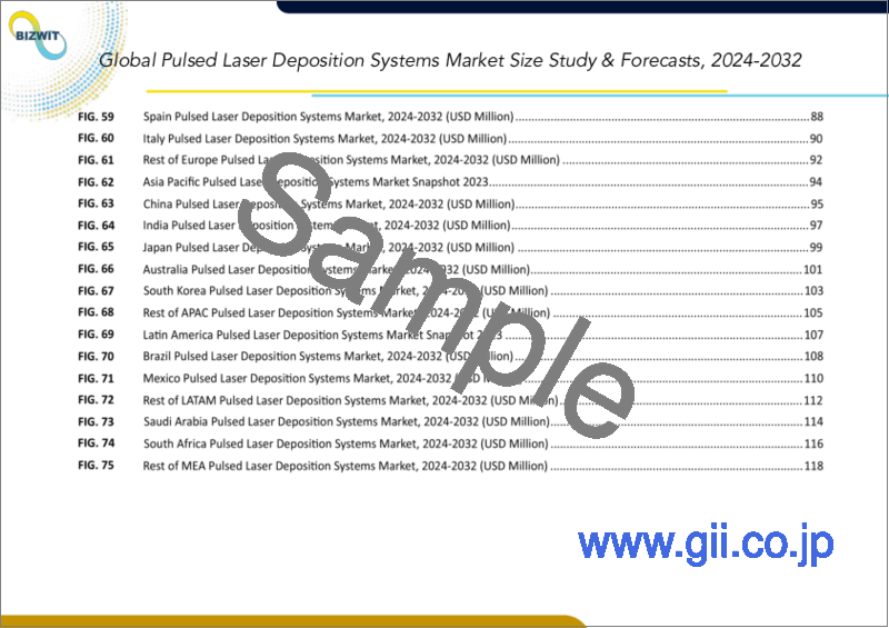
- FIG 14. Global Pulsed Laser Deposition Systems Market, regional snapshot 2020 & 2030
- FIG 15. North America Pulsed Laser Deposition Systems Market 2020 & 2030 (USD Billion)
- FIG 16. Europe Pulsed Laser Deposition Systems Market 2020 & 2030 (USD Billion)
- FIG 17. Asia pacific Pulsed Laser Deposition Systems Market 2020 & 2030 (USD Billion)
- FIG 18. Latin America Pulsed Laser Deposition Systems Market 2020 & 2030 (USD Billion)
- FIG 19. Middle East & Africa Pulsed Laser Deposition Systems Market 2020 & 2030 (USD Billion)
List of tables and figures and dummy in nature, final lists may vary in the final deliverable
Pulsed Laser Deposition (PLD) is a technique used for the fabrication and deposition of thin films and coatings. It involves the ablation of a target material using a high-energy pulsed laser, which creates a plasma plume consisting of vaporized target material. This plume is then condensed onto a substrate, forming a thin film with properties similar to the target material. In a typical PLD system, a high-energy pulsed laser beam is focused onto a target material placed in a vacuum chamber. The laser pulse vaporizes the target material, generating a plasma plume. The plume expands and deposits onto a heated substrate, where it cools down and forms a thin film. The process allows for precise control over the composition, stoichiometry, and structure of the deposited films. The rise in demand for renewable and sustainable energy around the globe is one of the primary factors driving the pulsed laser deposition systems market development. Furthermore, the advancements and innovations in the electronics and semiconductors industries have resulted in market growth.
Moreover, the PLD is a versatile technique used for depositing thin films of various materials, including semiconductors, oxides, and metals. These thin films are crucial in the manufacturing of electronic components such as integrated circuits (Ics), sensors, transistors, and capacitors. As the electronics industry continues to expand, there is an increasing demand for advanced materials and precise thin film deposition techniques like PLD. According to Statista, in 2019, the global electronics industry was valued at USD 495.40 billion; in 2022 the market reached USD 751.60 billion, and it is anticipated to reach USD 1180.70 billion by 2025. Additionally, growing technological advancement in pulsed laser deposition systems is anticipated to create lucrative opportunities for the market during forecast period. However, the high cost and integration of pulsed laser deposition systems stifles market growth throughout the forecast period of 2023-2030.
The key regions considered for the Global Pulsed Laser Deposition Systems Market study includes Asia Pacific, North America, Europe, Latin America, and Middle East & Africa. North America dominated the market in 2022 owing to the advancements in nanotechnology and material science, growing electronics industry, growing research and development (R&D) activities, and technological advancements and system innovations in the region. Whereas the Asia Pacific is expected to grow with the highest CAGR during the forecast period, owing to factors such as the growing demand in electronics and automotive industry, growing demand for advanced functional materials, government support and investments and rapid industrialization in the region.
Major market player included in this report are:
- PVD Products, Inc.
- PREVAC sp. Z.o.o.
- SVT Associates, Inc.
- Neocera
- Blue Wave Semiconductors
- Coherent, Inc.
- SURFACE systems + technology GmbH & Co. KG
- The Kurt J. Lesker Company
- Solmates
- Twente Solid State Technology BV
Recent Developments in the Market:
- NA
Global Pulsed Laser Deposition Systems Market Report Scope:
- Historical Data - 2020 - 2021
- Base Year for Estimation - 2022
- Forecast period - 2023-2030
- Report Coverage - Revenue forecast, Company Ranking, Competitive Landscape, Growth factors, and Trends
- Segments Covered - Design Type, Application, End User, Region
- Regional Scope - North America; Europe; Asia Pacific; Latin America; Middle East & Africa
- Customization Scope - Free report customization (equivalent up to 8 analyst's working hours) with purchase. Addition or alteration to country, regional & segment scope*
The objective of the study is to define market sizes of different segments & countries in recent years and to forecast the values to the coming years. The report is designed to incorporate both qualitative and quantitative aspects of the industry within countries involved in the study.
The report also caters detailed information about the crucial aspects such as driving factors & challenges which will define the future growth of the market. Additionally, it also incorporates potential opportunities in micro markets for stakeholders to invest along with the detailed analysis of competitive landscape and product offerings of key players. The detailed segments and sub-segment of the market are explained below:
By Design Type:
- Combinatorial PLD
- Nano PLD
- Others
By Application:
- Thin Film Preparations
- Solar Cells
- Others
By End User:
- Electronics
- Biotechnology
- Automotive
- Power
- Others
By Region:
- North America
- U.S.
- Canada
- Europe
- UK
- Germany
- France
- Spain
- Italy
- ROE
- Asia Pacific
- China
- India
- Japan
- Australia
- South Korea
- RoAPAC
- Latin America
- Brazil
- Mexico
- Middle East & Africa
- Saudi Arabia
- South Africa
- Rest of Middle East & Africa
Table of Contents
Chapter 1. Executive Summary
- 1.1. Market Snapshot
- 1.2. Global & Segmental Market Estimates & Forecasts, 2020-2030 (USD Billion)
- 1.2.1. Pulsed Laser Deposition Systems Market, by Region, 2020-2030 (USD Billion)
- 1.2.2. Pulsed Laser Deposition Systems Market, by Design Type, 2020-2030 (USD Billion)
- 1.2.3. Pulsed Laser Deposition Systems Market, by Application, 2020-2030 (USD Billion)
- 1.2.4. Pulsed Laser Deposition Systems Market, by End User, 2020-2030 (USD Billion)
- 1.3. Key Trends
- 1.4. Estimation Methodology
- 1.5. Research Assumption
Chapter 2. Global Pulsed Laser Deposition Systems Market Definition and Scope
- 2.1. Objective of the Study
- 2.2. Market Definition & Scope
- 2.2.1. Industry Evolution
- 2.2.2. Scope of the Study
- 2.3. Years Considered for the Study
- 2.4. Currency Conversion Rates
Chapter 3. Global Pulsed Laser Deposition Systems Market Dynamics
- 3.1. Pulsed Laser Deposition Systems Market Impact Analysis (2020-2030)
- 3.1.1. Market Drivers
- 3.1.1.1. Rise in Demand for Renewable and Sustainable Energy
- 3.1.1.2. Advanced Developments and Innovations in The Electronics and Semiconductors Industry
- 3.1.2. Market Challenges
- 3.1.2.1. High Cost Associated with Pulsed Laser Deposition Systems
- 3.1.3. Market Opportunities
- 3.1.3.1. Growing Technological Advancement
- 3.1.1. Market Drivers
Chapter 4. Global Pulsed Laser Deposition Systems Market Industry Analysis
- 4.1. Porter's 5 Force Model
- 4.1.1. Bargaining Power of Suppliers
- 4.1.2. Bargaining Power of Buyers
- 4.1.3. Threat of New Entrants
- 4.1.4. Threat of Substitutes
- 4.1.5. Competitive Rivalry
- 4.2. Porter's 5 Force Impact Analysis
- 4.3. PEST Analysis
- 4.3.1. Political
- 4.3.2. Economical
- 4.3.3. Social
- 4.3.4. Technological
- 4.3.5. Environmental
- 4.3.6. Legal
- 4.4. Top investment opportunity
- 4.5. Top winning strategies
- 4.6. COVID-19 Impact Analysis
- 4.7. Disruptive Trends
- 4.8. Industry Expert Perspective
- 4.9. Analyst Recommendation & Conclusion
Chapter 5. Global Pulsed Laser Deposition Systems Market, by Design Type
- 5.1. Market Snapshot
- 5.2. Global Pulsed Laser Deposition Systems Market by Design Type, Performance - Potential Analysis
- 5.3. Global Pulsed Laser Deposition Systems Market Estimates & Forecasts by Design Type 2020-2030 (USD Billion)
- 5.4. Pulsed Laser Deposition Systems Market, Sub Segment Analysis
- 5.4.1. Combinatorial PLD
- 5.4.2. Nano PLD
- 5.4.3. Others
Chapter 6. Global Pulsed Laser Deposition Systems Market, by Application
- 6.1. Market Snapshot
- 6.2. Global Pulsed Laser Deposition Systems Market by Application, Performance - Potential Analysis
- 6.3. Global Pulsed Laser Deposition Systems Market Estimates & Forecasts by Application 2020-2030 (USD Billion)
- 6.4. Pulsed Laser Deposition Systems Market, Sub Segment Analysis
- 6.4.1. Thin Film Preparations
- 6.4.2. Solar Cells
- 6.4.3. Others
Chapter 7. Global Pulsed Laser Deposition Systems Market, by End User
- 7.1. Market Snapshot
- 7.2. Global Pulsed Laser Deposition Systems Market by End User, Performance - Potential Analysis
- 7.3. Global Pulsed Laser Deposition Systems Market Estimates & Forecasts by End User 2020-2030 (USD Billion)
- 7.4. Pulsed Laser Deposition Systems Market, Sub Segment Analysis
- 7.4.1. Electronics
- 7.4.2. Biotechnology
- 7.4.3. Automotive
- 7.4.4. Power
- 7.4.5. Others
Chapter 8. Global Pulsed Laser Deposition Systems Market, Regional Analysis
- 8.1. Top Leading Countries
- 8.2. Top Emerging Countries
- 8.3. Pulsed Laser Deposition Systems Market, Regional Market Snapshot
- 8.4. North America Pulsed Laser Deposition Systems Market
- 8.4.1. U.S. Pulsed Laser Deposition Systems Market
- 8.4.1.1. Design Type breakdown estimates & forecasts, 2020-2030
- 8.4.1.2. Application breakdown estimates & forecasts, 2020-2030
- 8.4.1.3. End User breakdown estimates & forecasts, 2020-2030
- 8.4.2. Canada Pulsed Laser Deposition Systems Market
- 8.4.1. U.S. Pulsed Laser Deposition Systems Market
- 8.5. Europe Pulsed Laser Deposition Systems Market Snapshot
- 8.5.1. U.K. Pulsed Laser Deposition Systems Market
- 8.5.2. Germany Pulsed Laser Deposition Systems Market
- 8.5.3. France Pulsed Laser Deposition Systems Market
- 8.5.4. Spain Pulsed Laser Deposition Systems Market
- 8.5.5. Italy Pulsed Laser Deposition Systems Market
- 8.5.6. Rest of Europe Pulsed Laser Deposition Systems Market
- 8.6. Asia-Pacific Pulsed Laser Deposition Systems Market Snapshot
- 8.6.1. China Pulsed Laser Deposition Systems Market
- 8.6.2. India Pulsed Laser Deposition Systems Market
- 8.6.3. Japan Pulsed Laser Deposition Systems Market
- 8.6.4. Australia Pulsed Laser Deposition Systems Market
- 8.6.5. South Korea Pulsed Laser Deposition Systems Market
- 8.6.6. Rest of Asia Pacific Pulsed Laser Deposition Systems Market
- 8.7. Latin America Pulsed Laser Deposition Systems Market Snapshot
- 8.7.1. Brazil Pulsed Laser Deposition Systems Market
- 8.7.2. Mexico Pulsed Laser Deposition Systems Market
- 8.8. Middle East & Africa Pulsed Laser Deposition Systems Market
- 8.8.1. Saudi Arabia Pulsed Laser Deposition Systems Market
- 8.8.2. South Africa Pulsed Laser Deposition Systems Market
- 8.8.3. Rest of Middle East & Africa Pulsed Laser Deposition Systems Market
Chapter 9. Competitive Intelligence
- 9.1. Key Company SWOT Analysis
- 9.1.1. Company 1
- 9.1.2. Company 2
- 9.1.3. Company 3
- 9.2. Top Market Strategies
- 9.3. Company Profiles
- 9.3.1. PVD Products, Inc.
- 9.3.1.1. Key Information
- 9.3.1.2. Overview
- 9.3.1.3. Financial (Subject to Data Availability)
- 9.3.1.4. Product Summary
- 9.3.1.5. Recent Developments
- 9.3.2. PREVAC sp. z.o.o.
- 9.3.3. SVT Associates, Inc.
- 9.3.4. Neocera
- 9.3.5. Blue Wave Semiconductors
- 9.3.6. Coherent, Inc.
- 9.3.7. SURFACE systems + technology GmbH & Co. KG
- 9.3.8. The Kurt J. Lesker Company
- 9.3.9. Solmates
- 9.3.10. Twente Solid State Technology BV
- 9.3.1. PVD Products, Inc.
Chapter 10. Research Process
- 10.1. Research Process
- 10.1.1. Data Mining
- 10.1.2. Analysis
- 10.1.3. Market Estimation
- 10.1.4. Validation
- 10.1.5. Publishing
- 10.2. Research Attributes
- 10.3. Research Assumption