
VLSI製造における計測、検査、プロセス制御
Metrology, Inspection, and Process Control in VLSI Manufacturing- 発行日
- ページ情報
- 英文
- 納期
- 2~3営業日
- 商品コード
- 1479760
- 翻訳ツール提供対象 PDF対応AI翻訳ツールの無料貸し出しサービスのご利用が可能です
- 電子部品/半導体関連専門 電子部品/半導体関連専門を専門とする市場調査会社です。
概要
半導体計測と検査は、半導体デバイスの品質、信頼性、性能を保証する上で極めて重要な役割を担っています。この分野における進歩や投資は、いくつかの原動力によって推進されています。
全体として、半導体業界の絶え間ない技術革新の追求は、性能と品質への期待の高まりと相まって、計測・検査技術の絶え間ない進歩を促しています。これらのツールは、現代のエレクトロニクスを支える最先端半導体デバイスの開発と生産を可能にするために不可欠です。
半導体製造プロセスが複雑化するにつれて、リアルタイムのプロセス制御の必要性が高まっています。先進的な計測・検査システムにより、メーカーはプロセスを詳細に監視し、最適なパフォーマンスとスループットを確保するために即座に調整を行うことができます。このリアルタイム・フィードバック・ループは、精密製造と生産効率の微妙なバランスを維持するために不可欠です。
マイクロチップ上のトランジスタが約2年ごとに倍増し、同時にコストが低下するというムーアの法則の追求は、半導体デバイスの継続的な小型化をもたらしました。この微細化には、1ナノメートル以下の形状を評価できる高度な計測・検査技術が必要です。デバイスの微細化に伴い、わずかな欠陥やばらつきでもデバイスの性能に大きな影響を与える可能性があるため、精密で正確な測定は品質管理と歩留まり管理にとって非常に重要です。
半導体計測・検査技術における最近の技術革新は、半導体デバイスのサイズがますます小さくなり、その製造プロセスが複雑化することによってもたらされる課題に対処する上で、極めて重要なものとなっています。これらの進歩は、現代のエレクトロニクスの基幹である半導体部品の品質、性能、信頼性を確保するために不可欠です。
人工知能(AI)と機械学習(ML)は、欠陥検出と分類のスピード、精度、効率を向上させることで、半導体計測と検査に革命をもたらしています。これらの技術は、検査プロセス中に生成される膨大なデータの分析を可能にし、潜在的な欠陥や品質問題を示す可能性のあるパターンや異常を特定します。AIアルゴリズムは過去のデータから学習し、欠陥を予測・特定することができるため、手作業による検査にかかる時間とコストを削減し、歩留まりを向上させることができます。
当レポートでは、半導体検査・計測市場の包括的かつ詳細な分析を提供しています。広範な調査、業界の専門知識、市場の洞察に基づき、検査・計測分野の現状と将来見通しについて全体的な見解を提供します。
目次
第1章 イントロダクション
第2章 エグゼクティブサマリー
第3章 計測・検査技術
- イントロダクション
- イメージング技術
- 走査プローブ顕微鏡
- 光学技術
- フィルムの厚さと粗さ
第4章 欠陥レビュー/ウエハー検査
- イントロダクション
- 欠陥レビュー
- パターン付きウエハー検査
- パターンなしウエハー検査
- マクロ欠陥検査
第5章 薄膜計測
- イントロダクション
- 金属薄膜計測
- 非金属薄膜計測
- 基板/その他の薄膜計測
第6章 リソグラフィ計測
第7章 市場予測
- イントロダクション
- 市場予測の前提条件
- 市場予測
- トータルプロセス制御市場予測
- リソグラフィ計測市場予測
- ウエハ検査・欠陥レビュー市場
- 薄膜計測市場予測
- その他のプロセス制御システム市場予測
- バックエンド計測/検査市場予測
第8章 統合/現場計測/検査の動向
- イントロダクション
- In-Situ計測
- 統合計測
第9章 主な促進要因
- 3D
- バックエンド計測検査
- 300mm/450mmウエハ
- 銅の計測
- 低誘電率誘電体
- 化学機械平坦化(CMP)
- イオンインプラント
図表
List of Tables
- 3.1. Comparison Of Derivative AFM Techniques
- 5.1. Comparison Of White-Light With Multiple-Angle Laser Ellipsometry
- 7.1. Total Process Control Market Forecast
- 7.2. Lithography Metrology Market Forecast
- 7.3. Overlay Market Forecast
- 7.4. CD Measurement Market Forecast
- 7.5. Mask Inspection Market Forecast
- 7.6. Mask Metrology Market Forecast
- 7.7. Wafer Inspection / Defect Review Market Forecast
- 7.8. Patterned Wafer Inspection Market Forecast
- 7.9. E-Beam Patterned Wafer Inspection Market Forecast
- 7.10. Optical Patterned Wafer Inspection Market Forecast
- 7.11. Defect Review Market Forecast
- 7.12. SEM Defect Review Market Forecast
- 7.13. Optical Defect Review Market Forecast
- 7.14. Other Defect Review Market Forecast
- 7.15. Unpatterned Wafer Inspection Market Forecast
- 7.16. Macro Defect Detection Market Forecast
- 7.17. Thin Film Metrology Market Forecast
- 7.18. Non-Metal Thin Film Metrology Market Forecast
- 7.19. Non-Metal Standalone Thin Film Metrology Market Forecast
- 7.20. Non-Metal Integrated Thin Film Metrology Market Forecast
- 7.21. Substrate / Other Thin Film Metrology Market Forecast
- 7.22. Other Process Control Systems Market Forecast
- 9.1. Dielectric Film Challenges
List of Figures
- 3.1. Schematic Of Scanning Electron Microscope
- 3.2. Schematic Of Transmission Electron Microscope
- 3.3. Schematic Of Atomic Force Microscopy
- 3.4. Schematic Of Scanning Tunneling Microscopy
- 3.5. Interaction Between Two Atoms In AFM
- 3.6. Schematic Of Lateral Force Microscopy
- 3.7. Schematic Of Dynamic Force Mode AFM
- 3.8. Schematic Of Scanning Surface Potential Microscopy
- 3.9. Principle Of Scatterometry
- 3.10. Schematic Of Ellipsometer
- 3.11. Principles Of CD Scatterometry
- 3.12. Conventional TXRF Analysis Geometry
- 3.13. Schematic Of Secondary Ion Mass Spectrometry
- 3.14. Principle Of Auger Electron Emission
- 3.15. Schematic Of Auger Electron Spectroscopy
- 3.16. Schematic Of Focused Ion Beam Technology
- 3.17. Schematic Of X-Ray Reflectometry
- 3.18. Schematic Of X-Ray Photoelectron Spectroscopy
- 3.19. Schematic Of Rutherford Backscattering
- 3.20. Schematic Of Optical Acoustics Metrology
- 3.21. Spatial Wavelength Of Nanotopography
- 3.22. Schematic Of Non-Contact Capacitive Gauging
- 3.23. Schematic Of Stylus Profilometer
- 5.1. Spectroscopic Ellipsometry Diagram
- 6.1. ITRS Overlay Technology Roadmap
- 6.2. Illustration Of 3D Structure
- 6.3. ITRS Metrology Roadmap
- 6.4. Schematic Of OCD Optics
- 7.1. Total Process Control Market Forecast
- 7.2. Total Process Control Market By Geographic Region
- 7.3. Total Process Control Market Vs. Overall Equipment Market
- 7.4. Lithography Metrology Market Shares
- 7.5. Overlay Market Shares
- 7.6. CD Measurement Market Shares
- 7.7. Mask Inspection Market Shares
- 7.8. Mask Metrology Market Shares
- 7.9. Wafer Inspection / Defect Review Market Shares
- 7.10. Patterned Wafer Inspection Market Shares
- 7.11. E-Beam Patterned Wafer Inspection Market Shares
- 7.12. Optical Patterned Wafer Inspection Market Shares
- 7.13. Defect Review Market Shares
- 7.14. SEM Defect Review Market Shares
- 7.15. Optical Defect Review Market Shares
- 7.16. Other Defect Review Market Shares
- 7.17. Unpatterned Wafer Inspection Market Shares
- 7.18. Macro Defect Detection Market Shares
- 7.19. Thin Film Metrology Market Shares
- 7.20. Non-Metal Thin Film Metrology Market Shares
- 7.21. Non-Metal Standalone Thin Film Metrology Market Shares
- 7.22. Non-Metal Integrated Thin Film Metrology Market Shares
- 7.23. Substrate / Other Thin Film Metrology Market Shares
- 7.24. Other Process Control Systems Market Shares
- 7.25. Other Process Software Market Shares
- 8.1. Integrated Control In A Fab
- 9.1. Polish Endpoint Control
目次
Driving Forces
Semiconductor metrology and inspection play crucial roles in ensuring the quality, reliability, and performance of semiconductor devices. Several driving forces propel advancements and investments in this field.
Overall, the semiconductor industry's relentless pursuit of innovation, coupled with increasing performance and quality expectations, drives continuous advancements in metrology and inspection technologies. These tools are essential for enabling the development and production of cutting-edge semiconductor devices that power modern electronics.
Process Control and Throughput: As semiconductor manufacturing processes become more complex, the need for real-time process control increases. Advanced metrology and inspection systems enable manufacturers to monitor processes closely and make immediate adjustments to ensure optimal performance and throughput. This real-time feedback loop is essential for maintaining the delicate balance between precision manufacturing and production efficiency.
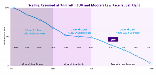
Technological Advancements and Miniaturization: The pursuit of Moore's Law, which predicts a doubling of transistors on a microchip approximately every two years while decreasing cost, has led to the continual miniaturization of semiconductor devices. This miniaturization necessitates advanced metrology and inspection techniques capable of characterizing features at the nanometer scale and below. As devices shrink, even the smallest defects or variations can have a significant impact on device performance, making precise and accurate measurements critical for quality control and yield management.
Complex 3D Structures and New Materials: The evolution of semiconductor devices includes not just shrinking sizes but also increasing complexity in device architecture, such as 3D NAND flash memory and FinFET transistors. These complex structures improve performance and storage capacity but introduce new challenges in measurement and inspection. Additionally, the integration of new materials with unique properties necessitates the development of novel metrology tools capable of accurately assessing material characteristics without damaging the delicate structures.
Yield Optimization: In the highly competitive semiconductor industry, optimizing yield-the percentage of devices on a wafer that function correctly-is crucial for economic viability. Metrology and inspection are integral to identifying process variations and defects early in the manufacturing process, allowing for adjustments that minimize waste and improve yield. The ability to precisely measure and control the production process leads to significant cost savings and higher profitability.
Quality and Reliability Standards: The end applications of semiconductor devices, particularly in critical areas such as automotive, medical, and aerospace industries, demand the highest levels of quality and reliability. This demand requires stringent quality control measures throughout the manufacturing process, supported by sophisticated metrology and inspection techniques. These tools ensure that devices meet the rigorous standards required for their intended applications, minimizing the risk of failures that could have severe consequences.
Innovation in Metrology and Inspection Technologies
Recent innovations in semiconductor metrology and inspection technologies have been pivotal in addressing the challenges posed by the ever-decreasing size of semiconductor devices and the complexity of their manufacturing processes. These advancements are critical for ensuring the quality, performance, and reliability of semiconductor components, which are the backbone of modern electronics. Here's an overview of some of the significant innovations in this field:
Artificial intelligence (AI) and machine learning (ML) are revolutionizing semiconductor metrology and inspection by improving the speed, accuracy, and efficiency of defect detection and classification. These technologies enable the analysis of vast amounts of data generated during the inspection process, identifying patterns and anomalies that may indicate potential failures or quality issues. AI algorithms can learn from historical data to predict and identify defects, reducing the time and cost associated with manual inspection and increasing yield rates.
High-resolution imaging techniques have seen substantial advancements, including electron microscopy (EM), atomic force microscopy (AFM), and X-ray tomography. These methods provide detailed views of semiconductor devices at the nanometer scale, allowing for precise characterization of features and defects. For instance, electron beam microscopy can now offer images at resolutions sufficient to inspect the atomic structure of materials, crucial for understanding complex 3D device architectures.
Multi-beam inspection systems use multiple electron beams simultaneously to inspect semiconductor wafers. This approach significantly increases throughput compared to traditional single-beam systems, enabling more comprehensive and faster inspections. Multibeam systems are particularly effective in identifying defects in complex patterns and multilayer structures, essential for ensuring the quality of advanced semiconductor devices.
Three-dimensional metrology technologies have become increasingly important for measuring the dimensions and profiles of complex 3D structures in semiconductor devices, such as FinFETs and 3D NAND flash memory. Techniques such as 3D X-ray microscopy (XRM) and 3D scanning electron microscopy (SEM) provide detailed volumetric measurements, offering insights into the quality and integrity of these structures.
The integration of metrology equipment directly into semiconductor fabrication tools allows for real-time process monitoring and control. This inline metrology approach enables immediate feedback and adjustments, reducing the cycle time for process optimization and significantly improving the efficiency of the manufacturing process. Integrated metrology systems utilize various measurement techniques, including optical, electrical, and material characterization methods, to ensure process stability and performance.
Advanced spectroscopic techniques, such as Raman spectroscopy and ellipsometry, have been refined for semiconductor metrology, providing non-destructive ways to analyze material properties, including composition, thickness, and refractive index. These techniques are invaluable for characterizing thin films, multi-layer stacks, and new materials being introduced in semiconductor manufacturing.
The use of big data analytics in semiconductor metrology and inspection involves processing and analyzing the vast amounts of data generated during the manufacturing process. This analysis helps identify trends, predict failures, and optimize manufacturing processes. Big data tools enable the correlation of data across different stages of production, improving overall yield and device performance.
Non-contact inspection methods, such as terahertz imaging and ultrasonic scanning, are being developed to inspect semiconductor wafers and devices without risking damage. These methods are particularly useful for inspecting delicate structures and materials, offering a safer alternative to traditional contact-based inspection techniques.
Need For This Report
In today's semiconductor industry, where innovation and precision are paramount, the importance of inspection and metrology cannot be overstated. As semiconductor devices continue to evolve at a rapid pace, with shrinking feature sizes, increasing complexity, and growing demands for reliability and performance, the need for robust inspection and metrology solutions has never been greater. These technologies serve as the cornerstone of quality assurance in semiconductor manufacturing, enabling the detection of defects, measurement of critical dimensions, and characterization of materials at the nanoscale level.
As the semiconductor landscape undergoes profound transformations driven by technological advancements, shifting market dynamics, and evolving customer requirements, staying abreast of the latest trends, developments, and challenges in inspection and metrology is essential for industry stakeholders. Whether you are a semiconductor manufacturer striving to optimize production processes, a supplier seeking to develop innovative solutions, a researcher exploring cutting-edge technologies, or an investor evaluating market opportunities, a comprehensive understanding of the semiconductor inspection and metrology landscape is indispensable.
Against this backdrop, this report offers a comprehensive and in-depth analysis of the semiconductor inspection and metrology market. Drawing on extensive research, industry expertise, and market insights, this report provides a holistic view of the current state and future prospects of the inspection and metrology sector. From emerging trends and technological innovations to competitive dynamics and growth opportunities, this report covers a wide range of topics essential for industry professionals and decision-makers.
Key areas of focus include the latest advancements in inspection and metrology technologies, market trends and drivers shaping industry growth, competitive landscape and key players' strategies, regulatory and standards landscape, and future outlook and growth prospects. By leveraging actionable insights and strategic recommendations provided in this report, stakeholders can gain a competitive edge, identify growth opportunities, mitigate risks, and make informed decisions to drive success in the dynamic and fast-paced semiconductor inspection and metrology market.
In summary, this report serves as an indispensable resource for anyone looking to navigate the complexities of the semiconductor inspection and metrology landscape. Whether you are seeking to understand market dynamics, evaluate competitive positioning, identify growth opportunities, or formulate strategic plans, this report equips you with the insights and analysis needed to succeed in the ever-evolving semiconductor industry.
About This Report
This 300-page report offers a complete analysis of the Process Control market, segmented as:
- Lithography Metrology
- Overlay (standalone)
- CD Measurement
- Mask Inspection
- Mask Metrology
- Wafer Insp/Defect
- Patterned Wafer Insp
- E-beam Patterned
- Optical Patterned
- Defect Review
- SEM Defect Review
- Optical Defect Review
- Other Defect Review
- Unpatterned Wafer Insp
- Macro Defect Detection
- Patterned Wafer Insp
- Thin Film Metrology
- Non-Metal Thin Film
- Non-Metal Standalone
- Non-Metal Integrated
- Substrate Metrology
- Non-Metal Thin Film
- Other Process Systems
- Other Process
- Software
- Back End
Includes excel spreadsheet of market revenues of each competitor in 22 segments from 2012 to 2023.
Table of Contents
Chapter 1. Introduction
Chapter 2. Executive Summary
Chapter 3. Metrology/Inspection Technologies
- 3.1. Introduction
- 3.2. Imaging Techniques
- 3.2.1. Scanning Electron Microscope (SEM)
- 3.2.2. Transmission Electron Microscope (TEM)
- 3.3. Scanning Probe Microscopes
- 3.3.1. Atomic Force Microscopy (AFM)
- 3.3.2. Scanning Tunneling Microscopy (STM)
- 3.3.3. Scanning Probe Microscopy (SPM)
- 3.3.4. AFM Types
- 3.3.4.1. Contact AFM
- 3.3.4.2. Dynamic Force Mode AFM Techniques
- 3.3.5. Scanning Surface Potential Microscopy (SSPM)
- 3.4. Optical Techniques
- 3.4.1. Scatterometry
- 3.4.1.1. Ellipsometry
- 3.4.1.2. Reflectometry
- 3.4.1.3. Scatterometry Developments
- 3.4.2. Total Reflection X-Ray Fluorescence (TXRF)
- 3.4.3. Energy Dispersive X-Ray Analysis (EDX)
- 3.4.4. Secondary Ion Mass Spectrometry (SIMS)
- 3.4.4.1. Surface Imaging Using SIMS
- 3.4.4.2. SIMS Depth Profiling
- 3.4.5. Auger Electron Spectroscopy
- 3.4.6. Focused Ion Beam (FIB)
- 3.4.7. X-Ray Reflectometry (XRR)
- 3.4.8. X-Ray Photoelectron Spectroscopy (XPS)
- 3.4.9. Rutherford Backscattering (RBS)
- 3.4.10. Optical Acoustics Metrology
- 3.4.11. Fourier Transform Infrared Spectroscopy (FTIR)
- 3.4.12. Thermally-Induced Voltage Alteration (TIVA)
- 3.4.1. Scatterometry
- 3.5. Film Thickness And Roughness
- 3.5.1. Surface Inspection Technology
- 3.5.2. Dimensional Technology
- 3.5.3. Stylus Profilometer
Chapter 4. Defect Review/Wafer Inspection
- 4.1. Introduction
- 4.2. Defect Review
- 4.2.1. SEM Defect Review
- 4.2.2. Optical Defect Review
- 4.2.3. Other Defect Review
- 4.3. Patterned Wafer Inspection
- 4.3.1. E-Beam Patterned Wafer Inspection
- 4.3.2. Optical Patterned Wafer Inspection
- 4.4. Unpatterned Wafer Inspection
- 4.5. Macro-Defect Inspection
Chapter 5. Thin Film Metrology
- 5.1. Introduction
- 5.1.1. Front End Applications
- 5.1.2. Back End Applications
- 5.2. Metal Thin-Film Metrology
- 5.3. Non-Metal Thin-Film Metrology
- 5.4. Substrate/Other Thin Film Metrology
Chapter 6. Lithography Metrology
- 6.1. Overlay
- 6.2. CD
- 6.3. Mask (Reticle) Metrology/Inspection
Chapter 7. Market Forecast
- 7.1. Introduction
- 7.2. Market Forecast Assumptions
- 7.3. Market Forecast
- 7.3.1. Total Process Control Market Forecast
- 7.3.2. Lithography Metrology Market Forecast
- 7.3.2.1. Overlay Market Forecast
- 7.3.2.2. CD Measurement Market Forecast
- 7.3.2.3. Mask Inspection Market Forecast
- 7.3.2.4. Mask Metrology Market Forecast
- 7.3.3. Wafer Inspection / Defect Review Market
- 7.3.3.1. Patterned Wafer Inspection Market Forecast
- E-Beam Patterned Wafer Inspection Market Forecast
- Optical Patterned Wafer Inspection Market Forecast
- 7.3.3.2. Defect Review Market Forecast
- SEM Defect Review Market Forecast
- Optical Defect Review Market Forecast
- Other Defect Review Market Forecast
- 7.3.3.3. Unpatterned Wafer Inspection Market Forecast
- 7.3.3.4. Macro Defect Detection Market Forecast
- 7.3.3.1. Patterned Wafer Inspection Market Forecast
- 7.3.4. Thin Film Metrology Market Forecast
- 7.3.4.1. Non-Metal Thin Film Metrology Market Forecast
- Non-Metal Standalone Thin Film Metrology Market Forecast
- Non-Metal Integrated Thin Film Metrology Market Forecast
- 7.3.4.2. Substrate / Other Thin Film Metrology Market Forecast
- 7.3.4.1. Non-Metal Thin Film Metrology Market Forecast
- 7.3.5. Other Process Control Systems Market Forecast
- 7.3.6. Back-End Metrology/Inspection Market Forecast
Chapter 8. Integrated/In-Situ Metrology/Inspection Trends
- 8.1. Introduction
- 8.2. In-Situ Metrology
- 8.3. Integrated Metrology
- 8.3.1. Benefits
- 8.3.2. Limitations
Chapter 9. Key Drivers
- 9.1. 3D
- 9.2. Back End Metrology Inspection
- 9.3. 300mm/450mm Wafers
- 9.4. Copper Metrology
- 9.5. Low-K Dielectrics
- 9.6. Chemical Mechanical Planarization (CMP)
- 9.7. Ion Implant
- 発行日
- 発行
- Information Network
- ページ情報
- 英文
- 納期
- 2~3営業日