|
|
市場調査レポート
商品コード
1408170
半導体レーザー-市場シェア分析、産業動向・統計、2024~2029年成長予測Semiconductor Laser - Market Share Analysis, Industry Trends & Statistics, Growth Forecasts 2024 - 2029 |
||||||
|
|
|||||||
|
● お客様のご希望に応じて、既存データの加工や未掲載情報(例:国別セグメント)の追加などの対応が可能です。 詳細はお問い合わせください。 |
|||||||

| 半導体レーザー-市場シェア分析、産業動向・統計、2024~2029年成長予測 |
|
出版日: 2024年01月04日
発行: Mordor Intelligence
ページ情報: 英文 120 Pages
納期: 2~3営業日
|
- 全表示
- 概要
- 目次
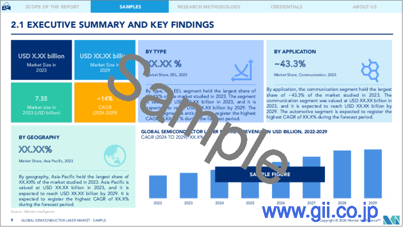
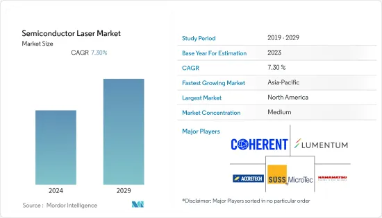
半導体産業向けレーザー市場は、2024年に80億2,000万米ドル、2029年には114億米ドルになると予測され、予測期間中のCAGRは7.3%で成長する見込み。
主要ハイライト
- レーザーは、半導体業界の厳しいニーズを満たす柔軟で発展的な加工を提供し、半導体メーカーに異なる材料から複雑な形態を高精度で切断する正確な方法を提供することから、半導体業界で大きな牽引力を獲得しています。半導体アプリケーション用にカスタム開発されたレーザーシステムは、さまざまな材料を正確かつ高速に切断することができます。
- 半導体市場は、活発な研究開発活動により、いくつかの技術革新を目の当たりにしています。例えば、2022年11月、フランスのLP3研究所の研究者は、半導体チップの3D空間内で局所的な材料加工を実現する直接レーザー書き込み技術を開発しました。研究者らは、半導体製造部門が抱える課題に徹底的に対処するには、主要な製造技術であるリソグラフィには大きな限界があると主張しています。このため、ウエハー表面下に構造を作製し、材料内部の空間全体を利用することが非常に望ましいとしています。International Journal of Extreme Manufacturing』誌において、研究者らは、新設計の直接レーザー描画技術により、このような機能を実証しました。
- さらに、2022年6月、カリフォルニア大学バークレー校(電気工学・コンピューター科学科(EECS))のエンジニアは、光学分野におけるとらえどころのない目標、すなわち、サイズとパワーを拡大する能力を維持しながら、放射される光の単一モードを維持する能力を完成させる、新しいタイプの半導体レーザーを設計しました。これは、サイズがコヒーレンスを犠牲にする必要がないことを意味し、レーザーがより強力になり、多くの用途でより長い距離をカバーできるようになるという重要な成果です。
- 調査された市場は、様々な国の政府による数多くのイニシアチブのために需要の増加に気づいています。例えば、米国政府は半導体サプライチェーンのエコシステムで独立することを目指しています。このような目標を実現するため、米国政府はイニシアチブを取り始めています。例えば米国政府は最近、国内半導体製造への投資法を上院に提出しました。この法案では、半導体業界向けの政府補助金プログラムであるCHIPS for Americaの対象を拡大し、半導体の製造、試験、組立、研究開発に携わる企業だけでなく、半導体の製造に使用される材料や半導体製造装置に携わる企業にも資金援助を行う。必要不可欠な材料や装置を生産する企業にインセンティブを与えることで、本法案は全国の製造業者により多くの機会を創出し、国内の半導体製造を支えるサプライチェーンを強化することができます。
- さらに2022年9月、バイデン政権は中国依存に対抗するため、国内半導体産業の育成に500億米ドルを投資すると発表しました。米国は国家安全保障に不可欠な世界の最先端チップのうち、生産量ゼロ、消費量25%を占めているからです。ジョー・バイデン大統領は2022年8月、中国に対する米国の競合強化の一環として、国内のハイテク製造業を後押しする2,800億米ドルのCHIPS法案に署名しました。この地域の半導体セクターへのこのような力強い投資は、研究市場の成長にとって有利な機会を生み出すと思われます。
- しかし、その反面、レーザーの初期校正は非常に複雑な作業であり、アプリケーションに必要な高精度のチューニングを実現するには高度な専門知識が必要となります。また、レーザーのチューニング中には膨大な数のパラメーターを考慮しなければならず、わずかなオフセットがエラーにつながったり、様々な用途で致命的な影響を及ぼす可能性があります。レーザーの製造工程は非常に複雑で、そのため製造コストも大幅に上昇しています。波長切り替え時のレーザー性能のもう一つの重要な点は、デバイスの波長の安定性です。レーザーが希望の波長にチューニングされると、チャネルが最終的に安定する前にセトリング・ドリフトが現れます。このような要因が、研究対象市場の成長を妨げる可能性があります。
- さらに、半導体製造はコストと時間のかかるプロセスであり、関係するすべての装置/プロセスにおいて熾烈な精度が要求されます。その結果、経済的に発展していない地域では産業の拡大が制限されます。半導体産業に不可欠なコンポーネントの一つであるレーザーもまた、調査された市場の成長を鈍らせる同様の課題に直面しています。
半導体レーザー市場動向
検査・計測セグメントが主要市場シェアを占める見込み
- スマートフォンや家電、自動車などの用途は、高性能で低コストの半導体チップの必要性を高めています。ワイヤレス技術(5G)、人工知能など、技術の変遷がこれらの産業を後押ししています。また、モノのインターネット(IoT)機器の増加動向は、スマート製品実現のためのこの機器への投資を半導体業界を後押しすると予想されます。
- さらに、デジタル化の進展や遠隔作業・運用の動向は、様々な新機能を可能にする高度な半導体デバイスへの要求に火をつけています。半導体デバイスへのニーズが一貫して強まる中、先進パッケージング技術は、今日のデジタル化された世界に必要なフォームファクターと処理能力を提供します。半導体産業協会(SIA)によると、2022年8月の世界半導体産業売上高は474億米ドルで、2021年8月の473億米ドルから0.1%の微増でした。このような半導体需要の拡大は、検査・計測機器の成長に有利な機会を提供すると予想されます。
- さらに、半導体業界の生産能力開拓も新興国市場の成長を後押ししています。例えば、SEMI Equipment Market Data Subscription(EMDS)によると、半導体業界の足元はしっかりとアクセルを踏んでおり、生産能力拡大の努力も、成長促進要因を満たすために前工程と後工程の半導体装置産業の拡大を助けています。
- 2023年第1四半期の半導体製造装置の売上高は、前年同期比9%増の268億米ドルとなった。先端ロジックとファウンドリの生産能力拡大、DRAM投資の回復、堅調なNANDフラッシュ投資が装置市場の成長を牽引しました。計測と検査は半導体チップの製造に関わる重要なプロセスであるため、このような動向もレーザー市場に有利な展望を生み出しています。
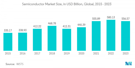
- さらにWSTSによると、2022年、半導体売上は世界で5,801億3,000万米ドルに達します。半導体は電子機器において極めて重要であり、この業界は競争が激しいです。2022年の前年比成長率は4.4%に達し、今後さらに成長すると予測されています。このような動向は、予測期間中、計測・検査装置と関連レーザーシステムの成長をサポートすると予測されています。
高い市場成長が期待されるアジア太平洋
- アジア太平洋は、半導体産業の製造と消費の主要地域の一つです。Semiconductor Equipment and Materials International(SEMI)によると、中国の半導体装置支出額は2022年に282億7,000万米ドルを突破しました。さらに韓国では215億1,000万米ドル、台湾では268億2,000万米ドルが同期間に支出されました。レーザーは半導体装置に広く使用されているため、このような動向は市場の成長に有利です。
- この地域はまた、半導体産業を後押しする政府による多くのイニシアチブを誇っています。例えば、中国政府の国家集積回路産業発展ガイドラインとメイド・イン・チャイナ2025イニシアチブは、国内の半導体産業の成長を強化し、他国への依存度を下げることを目的としています。
- 同様の動向は他国でも見られます。例えば、インドの電子情報技術省(MeitY)は最近、半導体・ディスプレイ製造エコシステム開発のための包括的なPLIスキームを承認しました。今後6年間で7,600億インドルピー(98億1,000万米ドル)相当の奨励金が交付される予定です。この地域のこのようなイニシアチブは、半導体産業のエコシステムの成長を促進し、レーザー市場にも機会を創出すると期待されています。
- 半導体は、自動車、スマートフォン、ロボット、その他多くのインテリジェント・デバイスなどの最新機器に統合されたエレクトロニクスの基幹材料であり続けています。小型化された堅牢なチップへの継続的なニーズによって、現在の半導体製造技術はますます大きな圧力に直面しています。アジア太平洋では、家電や自動車の採用が増加しており、調査対象市場の成長に有利な展望となっています。
- 日本は、半導体装置と材料の主要サプライヤーのひとつであり、調査市場においてユニークな位置を占めています。SEMIによると、日本は世界の半導体製造装置・材料売上の30%以上を占めています。したがって、日本は半導体産業で使用されるレーザーの注目すべき成長機会を保持すると予想されます。
- 近年、アジア太平洋では半導体のニーズが大きく伸びています。いくつかの国の著名な半導体顧客がサプライチェーンを強化するにつれて、半導体産業バリューチェーンへの投資はさらに加速しています。例えば、2022年7月、主に半導体リソグラフィに使用される光源メーカーのGigaphotonInc.は、日本に新棟を建設し、生産能力を2.5倍に増強すると発表しました。同社は新施設の建設に約50億円(3,620万米ドル)を投資し、2023年6月までに完成する予定です。このような投資は、半導体業界のレーザー市場拡大を後押しすると思われます。
半導体レーザー産業概要
半導体産業向けレーザー市場は、Lumentum Operations、Trumpf、SUSS MicroTec、Coherentなどの有力企業が存在する中程度の競争市場です。市場参入企業は、顧客の進化する要求に応えるために先進的な製品とプロセスの革新に努めています。
- 2023年3月-タワーセミコンダクターはQuintessent, Incと共同で、GaAs量子ドット(QD)レーザーとファウンドリシリコンフォトニクスプラットフォーム(PH18DB)の世界初の異種集積化を発表しました。このPH18DBプラットフォームは、データセンターと通信ネットワークの光トランシーバモジュールや、人工知能(AI)、機械学習、LiDAR、その他のセンサにおける新たな新興アプリケーションを対象としています。この新しいプラットフォームは、低損失導波路、光検出器、変調器を1つのシリコンチップ上にヘテロジニアスに集積したタワーの量産ベースPH18Mシリコンフォトニクスファウンドリー技術に基づいて作成されたGaAsベースの量子ドットレーザーと半導体光増幅器(SOA)を提供します。このプラットフォームにより、高密度フォトニック集積回路(PIC)が小型フォームファクタで高チャネル数を支援できます。
- 2023年1月-Coherent Corp.は、シングルチップで業界最高出力50Wを実現する次世代ポンプレーザーダイオードのイントロダクションを発表しました。切断、溶接、マーキング、積層造形などの材料加工用途へのファイバーレーザーの導入は加速しており、ワット当たりの出力コストを下げるキーコンポーネントの必要性が高まっています。この新しいレーザーダイオードの出力は50Wに達し、従来製品より40%高いため、少ないポンプレーザーダイオードで高出力産業用ファイバーレーザーの設計が可能になります。
その他の特典:
- エクセル形式の市場予測(ME)シート
- 3ヶ月間のアナリストサポート
目次
第1章 イントロダクション
- 調査の前提条件と市場定義
- 調査範囲
第2章 調査手法
第3章 エグゼクティブサマリー
第4章 市場洞察
- 市場概要
- マクロ動向が市場に与える影響
- 業界の魅力度-ポーターのファイブフォース分析
- 新規参入業者の脅威
- 買い手の交渉力
- 供給企業の交渉力
- 代替品の脅威
- 競争企業間の敵対関係
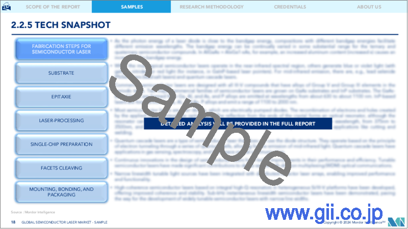
- 技術スナップショット
第5章 市場力学
- 市場促進要因
- 半導体製造工場への投資拡大
- 市場抑制要因
- レーザーの設計の複雑さとコスト
第6章 市場セグメンテーション
- レーザータイプ別
- ナノ秒
- ピコ秒
- CO2
- その他(フェムト秒、エキシマ)
- 加工ステップ別
- 除去プロセス
- 接着プロセス
- 検査・計測
- 改質プロセス
- 地域別
- 北米
- 欧州
- アジア太平洋
- その他
第7章 競合情勢
- Laser Equipment Suppliers Analysis
- Accretech
- Disco Corporation
- Coherent, Inc.
- IPG Photonics Corporation
- Veeco Instruments Inc.
- EVG Group
- SUSS MicroTec
- Orbotech/SPTS
- HGTech
- QMC
- Screen Semiconductor Solutions Co., Ltd.
- Nikon
- Laser Source Suppliers Analysis
- Micromac
- Lumentum Operations LLC
- Trumpf
- HANS Laser
- Amplitude Laser
- IPG
- Hamamatsu
- Ushio
- Jenoptik
- EO Technics
- HGTech
- Edgewave
- MKS
第8章 レーザー機器メーカーのベンダーランキング分析
第9章 市場の将来展望
The Laser Market for the Semiconductor Industry market is anticipated to be valued at USD 8.02 billion in 2024 and is expected to become 11.4 billion by 2029, growing at a CAGR of 7.3% during the forecast period.
Key Highlights
- Lasers are attaining significant traction in the semiconductor industry as they present flexible, developed machining to fulfill the stringent needs of the industry, delivering semiconductor manufacturers with an exact method of cutting complex shapes from different materials with high precision. A laser system custom-developed for semiconductor applications can cut a range of materials accurately and fast.
- The semiconductor market is witnessing several innovations owing to robust R&D activities. For instance, in November 2022, researchers from the LP3 Laboratory in France developed a direct laser writing technique to achieve local material processing within the 3D space of semiconductor chips. They claim that the dominating manufacturing technology, lithography, has significant limitations in thoroughly addressing the challenges posed by the semiconductor manufacturing sector. For this reason, fabricating structures under the wafer surfaces would be highly desirable to use the whole space inside the materials. In the International Journal of Extreme Manufacturing, the researchers demonstrated such capability via the newly designed direct laser writing technique, which facilitates fabricating implanted structures inside different semiconductor materials.
- Further, in June 2022, engineers at the University of California, Berkeley (Department of Electrical Engineering and Computer Sciences (EECS)) designed a new type of semiconductor laser that completes an elusive goal in the field of optics: the ability to sustain a single mode of emitted light while retaining the ability to scale up in size and power. It is a significant achievement as it means size does not have to come at the cost of coherence, allowing lasers to become more powerful and cover longer distances for many applications.
- The studied market is noticing an increase in demand due to numerous initiatives by governments of various nations. For instance, the United States government aims to become independent in the semiconductor supply chain ecosystem. To realize such goals, the United States government has started taking initiatives. Such as the US government recently introduced Investing in Domestic Semiconductor Manufacturing Act in the Senate. This proposed legislation would expand eligibility for CHIPS for America, a government subsidy program for the semiconductor industry, to fund financial assistance beyond entities involved in semiconductor fabrication, testing, assembly, or R&D to organizations involved with materials used to manufacture semiconductors and semiconductor manufacturing equipment. By incentivizing the companies that produce essential materials and equipment, this legislation can create more opportunities for manufacturers nationwide and strengthen the supply chain supporting domestic semiconductor manufacturing.
- Additionally, in September 2022, the Biden administration announced that it would invest USD 50 billion in building up the domestic semiconductor industry to counter dependency on China, as the US produces zero and consumes 25% of the world's leading-edge chips vital for its national security. President Joe Biden signed a USD 280 billion CHIPS bill in August 2022 to boost domestic high-tech manufacturing, part of his administration's push to increase US competitiveness over China. Such robust investments in the semiconductor sector in the region would create lucrative opportunities for the growth of the studied market.
- However, on the Flipside, the initial calibration of lasers is a very complex task and requires a high level of expertise to achieve the high-precision tuning needed for the application. Also, the vast number of parameters has to be considered while tuning the laser, and a small offset may lead to errors or be catastrophic in various applications. The manufacturing process of the lasers is very complex, due to which the manufacturing cost has also increased significantly. Another important aspect of the laser's performance when switching between wavelengths is the stability of the wavelength of the device. As the laser tunes into its desired wavelength, settling drift appears before the channel finally stabilizes. Such factors might hinder the growth of the studied market.
- Furthermore, semiconductor manufacturing is a costly and time-consuming process and requires cutthroat precision in all the equipment/processes involved. As a result, industry expansion is limited in economically less developed regions. Lasers, being one of the integral components of the semiconductor industry, also face similar challenges that slow down the studied market's growth.
Semiconductor Laser Market Trends
The Inspection & Metrology Segment is Expected to Hold a Major Market Share
- Smartphones & other applications across consumer electronics, automotive applications, etc., drive the need for high-performance, low-cost semiconductor chips. Technology transitions have encouraged these industries, including wireless technologies (5G), Artificial Intelligence, etc. Also, the trend of growing Internet of Things (IoT) devices is expected to push the semiconductor industry to invest in this equipment to achieve smart products.
- Moreover, the increasing digitization and trends of remote work and operations have sparked the requirement for advanced semiconductor devices that allow various new capabilities. As the need for semiconductor devices intensifies consistently, advanced packaging techniques deliver the form factor and processing power needed for today's digitized world. According to the Semiconductor Industry Association(SIA), during August 2022, global semiconductor industry sales were USD 47.4 billion, a slight increase of 0.1% over the August 2021 total of USD 47.3 billion. Such an expansion in the semiconductor requirement is anticipated to offer lucrative opportunities for the growth of inspection and metrology equipment.
- Furthermore, capacity developments in the semiconductor industry are also aiding the growth of the studied market. For instance, according to SEMI Equipment Market Data Subscription (EMDS), the semiconductor industry's foot is firmly on the accelerator as the capacity expansion efforts are also aiding the expansion of the front-end and back-end semiconductor equipment industries to meet growth drivers.
- Billings for semiconductor equipment in the first quarter of 2023 increased 9% year-over-year to USD 26.8 billion. Advanced logic and foundry capacity expansions, DRAM investment recovery, and robust NAND Flash spending drove equipment market growth. As metrology and inspection are crucial processes involved in the manufacturing of semiconductor chips, such trends also create a favorable outlook for the laser market.
- Further, according to WSTS, in 2022, semiconductor sales reached USD 580.13 billion worldwide. Semiconductors are crucial in electronic devices, and the industry is highly competitive. The YoY growth rate in 2022 reached 4.4 percent and is anticipated to grow more in the coming future. Such trends are anticipated to support the growth of metrology and inspection equipment and associated laser systems during the forecast period.
The Asia Pacific Region is Expected to Witness a High Market Growth
- The Asia-Pacific is one of the main regions for the semiconductor industry's manufacturing and consumption. According to Semiconductor Equipment and Materials International (SEMI), China's semiconductor equipment spending surpassed USD 28.27 billion in 2022. Moreover, in South Korea, spending amounted to USD 21.51 billion, while in Taiwan, it stood at USD 26.82 billion during the same period. As lasers are widely used in semiconductor equipment, such trends favor the studied market's growth.
- The region also boasts many initiatives by governments to boost the semiconductor industry. For instance, the Chinese government's National Integrated Circuit Industry Development Guidelines and the Made in China 2025 initiative aim to bolster the growth of the local semiconductor industry in the country, reducing the level of dependence on other countries.
- A similar trend is being observed across other countries. For instance, India's Ministry of Electronics and Information Technology (MeitY) recently approved a comprehensive PLI scheme for developing semiconductor & display manufacturing ecosystems. Incentives worth INR 76,000 crore (USD 9.81 billion) are to be distributed over the next six years. Such initiatives in the region are expected to drive the growth of the ecosystem of the semiconductor industry, creating opportunities in the laser market as well.
- Semiconductors remain the backbone material of electronics integrated with modern devices such as cars, smartphones, robots, and many other intelligent devices; driven by the continuous need for miniaturized and robust chips, current semiconductor manufacturing technologies face increasing pressure. The growing adoption of consumer electronics and automobiles in the Asia Pacific region also creates a favorable outlook for the growth of the studied market.
- Japan holds a unique place in the studied market as the country is among the leading suppliers of semiconductor equipment and materials. According to SEMI, Japan accounts for more than 30% of the global semiconductor manufacturing equipment and material sales. Hence, the country is anticipated to hold notable growth opportunities for lasers used in the semiconductor industry.
- The semiconductor need has grown significantly in the Asia Pacific region in recent years. As prominent semiconductor customers in several countries strengthen their supply chains, investments in the semiconductor industry value chain are further accelerated. For instance, in July 2022, GigaphotonInc., a manufacturer of light sources used primarily in semiconductor lithography, announced that it would increase its production capacity by 2.5 times by constructing a new building in Japan. The company invested around JPY 5 billion (USD 36.2 million) in the construction of the new facility, which is expected to be completed by June 2023. Such investments would boost the semiconductor industry's expansion of the laser market.
Semiconductor Laser Industry Overview
The Laser Market for Semiconductor Industry is a moderately competitive market with significant players like Lumentum Operations, Trumpf, SUSS MicroTec, Coherent, etc. The market players are striving to innovate advanced products and processes to cater to the evolving demands of their customers.
- March 2023 - Tower Semiconductor, in collaboration with Quintessent, Inc, announced the world's first heterogeneous integration of GaAs quantum dot (QD) lasers and a foundry silicon photonics platform (PH18DB). This PH18DB platform targets optical transceiver modules in data centers & telecom networks and new emerging applications in artificial intelligence (AI), machine learning, LiDAR, and other sensors. The new platform offers GaAs-based quantum dot lasers & semiconductor optical amplifiers (SOA) created on Tower's high-volume base PH18M silicon photonics foundry technology containing low-loss waveguides, photodetectors, & modulators heterogeneously integrated on a single silicon chip. This platform allows dense photonic integrated circuits (PICs) to assist higher-channel count in small form factors.
- January 2023 - Coherent Corp. announced the introduction of its next-generation pump laser diodes that execute an industry-record high output power of 50 W from a single chip. The deployment of fiber lasers for materials processing applications like cutting, welding, marking, and additive manufacturing is accelerating, driving the need for key components that lower the output power cost per watt. The new laser diodes reach 50 W of output power, 40% more than the existing product, allowing high-power industrial fiber laser designs with fewer pump laser diodes.
Additional Benefits:
- The market estimate (ME) sheet in Excel format
- 3 months of analyst support
TABLE OF CONTENTS
1 INTRODUCTION
- 1.1 Study Assumptions and Market Definition
- 1.2 Scope of the Study
2 RESEARCH METHODOLOGY
3 EXECUTIVE SUMMARY
4 MARKET INSIGHTS
- 4.1 Market Overview
- 4.2 Impact of Macro Trends on the Market
- 4.3 Industry Attractiveness - Porter's Five Forces Analysis
- 4.3.1 Threat of New Entrants
- 4.3.2 Bargaining Power of Buyers
- 4.3.3 Bargaining Power of Suppliers
- 4.3.4 Threat of Substitute Products
- 4.3.5 Intensity of Competitive Rivalry
- 4.4 Technology Snapshot
5 MARKET DYNAMICS
- 5.1 Market Drivers
- 5.1.1 Growing Investment in Semiconductor Fabrication Plants
- 5.2 Market Restraints
- 5.2.1 Desing Complexity and Cost of Lasers
6 MARKET SEGMENTATION
- 6.1 By Laser Type
- 6.1.1 Nanosecond
- 6.1.2 Picosecond
- 6.1.3 CO2
- 6.1.4 Others (Femtosecond and Excimer)
- 6.2 By Process Step
- 6.2.1 Removal Process
- 6.2.2 Bonding Process
- 6.2.3 Inspection & Metrology
- 6.2.4 Reforming Process
- 6.3 By Geography
- 6.3.1 North America
- 6.3.2 Europe
- 6.3.3 Asia Pacific
- 6.3.4 Rest of the World
7 COMPETITIVE LANDSCAPE
- 7.1 Laser Equipment Suppliers Analysis
- 7.1.1 Accretech
- 7.1.2 Disco Corporation
- 7.1.3 Coherent, Inc.
- 7.1.4 IPG Photonics Corporation
- 7.1.5 Veeco Instruments Inc.
- 7.1.6 EVG Group
- 7.1.7 SUSS MicroTec
- 7.1.8 Orbotech/SPTS
- 7.1.9 HGTech
- 7.1.10 QMC
- 7.1.11 Screen Semiconductor Solutions Co., Ltd.
- 7.1.12 Nikon
- 7.2 Laser Source Suppliers Analysis
- 7.2.1 Micromac
- 7.2.2 Lumentum Operations LLC
- 7.2.3 Trumpf
- 7.2.4 HANS Laser
- 7.2.5 Amplitude Laser
- 7.2.6 IPG
- 7.2.7 Hamamatsu
- 7.2.8 Ushio
- 7.2.9 Jenoptik
- 7.2.10 EO Technics
- 7.2.11 HGTech
- 7.2.12 Edgewave
- 7.2.13 MKS