 |
市場調査レポート
商品コード
1404474
原子層堆積装置:市場シェア分析、産業動向と統計、2024~2029年の成長予測Atomic Layer Deposition Equipment - Market Share Analysis, Industry Trends & Statistics, Growth Forecasts 2024 - 2029 |
||||||
● お客様のご希望に応じて、既存データの加工や未掲載情報(例:国別セグメント)の追加などの対応が可能です。 詳細はお問い合わせください。

| 原子層堆積装置:市場シェア分析、産業動向と統計、2024~2029年の成長予測 |
|
出版日: 2024年01月04日
発行: Mordor Intelligence
ページ情報: 英文 120 Pages
納期: 2~3営業日
|
- 全表示
- 概要
- 目次
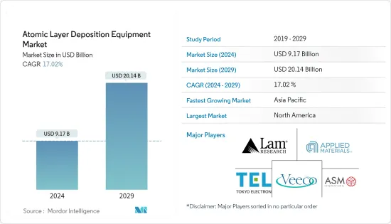
原子層堆積装置市場規模は2024年に91億7,000万米ドルと推定され、2029年には201億4,000万米ドルに達すると予測され、予測期間中(2024~2029年)にCAGR 17.02%で成長する見込みです。
世界の原子層堆積市場の拡大を後押ししている主要要因の1つは、世界中でエレクトロニクスと半導体ソリューションの採用が増加していることです。
主要ハイライト
- チップ生産向上のための新しい材料や設計の採用が、原子層堆積ソリューションの需要を促進しています。小型化の動向は世界中の産業で受け入れられています。その結果、小型の電子機器や機械に対するニーズが高まっています。
- Ciscoによると、2030年までに約5,000億台の機器がインターネットに接続されます。各機械には、データを収集し、環境と相互作用し、ネットワークを介して通信するセンサーが含まれています。これらの用途には、小型化されたストレージ・デバイスやICが必要です。接続される機器の増加から生成されるデータ量が増加することで、ストレージ・デバイスの需要が高まり、市場の成長を牽引しています。
- CMOSプロセッサー、メモリーデバイス、MEMS、センサーに使用される高誘電率膜は、半導体業界でALDを使用して頻繁に製造されています。燃料電池や耐腐食性・耐摩耗性を必要とするその他の用途における機能性・保護膜の作成には、ALD技術が使用されています。次世代デバイスの開発では、ナノワイヤーやナノチューブのような高アスペクト比構造のコーティングにも利用されています。
- 銅電極、高誘電体ゲートスタック、銅バリア/シード層など、半導体を作るためにさまざまな成膜ツールが使われています。例えば、インド商工省の一部である国家投資促進・円滑化庁が2022年3月に発表したデータによると、インドのエレクトロニクスの国内生産は2014~15年の290億米ドルから2020~2021年には670億米ドルに増加しました。
- さらに、ロボットの使用と製造の自動化が進めば、半導体の売上が増加し、ALD技術の市場が促進されると予想されています。産業オートメーションは現在、実質的にすべての重要な生産産業の性質を変えつつあります。インダストリー4.0規格の採用や、データ分析のための協働ロボット、AR/VR、AIの利用の増加は、ALD市場に利益をもたらすと予想されます。
- さらに、ALD薄膜層はマイクロエレクトロニクスにおいて、ナノスケールトランジスタの隣接部品を電気的にシールドするために利用される可能性があります。ALDは特に、複雑な3次元表面に正確なナノスケールコーティングを施すのに長けています。例えば、最新のコンピューター・プロセッサーの製造に使われるシリコンウエハーにエッチングされた深くて狭いトレンチのようなものです。このため、世界中の研究者は、今後の半導体デバイス世代に向けた新しい薄膜ALD材料の創製に意欲を燃やしています。
- 予測される期間中、研究開発に必要な高額の投資が世界の原子層堆積市場の成長を抑制すると予想されます。ALDは、そのアプローチに時間がかかるため、大きな制約があると認識されています。
- 原子層堆積業界のサプライチェーンは、COVID-19の流行により依然として苦しんでいます。COVID-19ウイルスは多くの国に大きな影響を与えています。労働力不足と原料供給の混乱により、パンデミックは原子層堆積材料の生産を妨げています。このような国際貿易の混乱により、進行中のプロジェクトの開発が遅れ、資本支出(CAPEX)が増加し、原子層堆積の供給が停止しました。
原子層堆積装置市場動向
半導体・エレクトロニクス産業が市場成長を牽引
- 半導体・エレクトロニクス産業からの需要が、原子層堆積技術の主要原動力になると予想されます。半導体産業がこの技術の発展に直接影響を与えると予想される一方で、エレクトロニクス産業の拡大はその進歩に寄与します。その結果、原子層堆積装置の需要が高まっています。
- チップ不足の結果としてメーカーが発表した世界のファブ生産能力拡大の後、原子層堆積(ALD)参入企業は新たな成長機会を利用する準備をしています。最近、300mm ALDプラットフォームは、More-than-Moore(MtM)デバイスや、MEMS、センサー、パワーとRFデバイス、フォトニクスなどの用途の要件を満たすために改良されてきました。以前は、200mm ALDプラットフォームが市場のニーズを満たすように設計されていました。ウエハー生産量が増加した現在、ALDソリューションが拡大し、MtMデバイス市場に加わることが期待されています。
- ALDが半導体産業で脚光を浴びるようになったのは、高誘電率の酸化物材料を成膜するためです。例えば、従来の金属酸化物半導体電界効果トランジスタのゲート絶縁材料として、熱成長させたSiO2をALDで形成したHfO2に置き換えました。ALDの使用を必要とする用途の数は、近年著しく増加しています。
- エレクトロニクス分野は、周期的に浮き沈みがあります。エレクトロニクス産業の短中期展望は明るいです。2024年までに、モバイル契約数は約89億件、モバイルブロードバンド契約数は約84億件、ユニークモバイルユーザー数は約62億人になると、エリクソンのモビリティレポートは予測しています。これにより、ALD技術の開発が加速すると予想されます。
- 予測期間中、民生用電子機器とマイクロエレクトロニクスの売上が伸び、半導体ICの需要が増加すると予想されます。半導体ICの需要増加は、半導体デバイスメーカーの製造能力を引き上げ、原子層堆積装置市場の需要を増加させる可能性があります。
- 次世代半導体デバイスの製造には、高アスペクト比のナノ構造上に、低温(400℃)で高コンフォーマル(95%以上)のSiO2、SiNx、SiC膜を成膜する必要があります。原子層堆積法は、半導体製造における化学堆積法に取って代わりつつあり、このようなSiベースの誘電体膜の開発を可能にしています。ALD堆積SiO2膜は、すでに半導体デバイスの製造に利用されています。
- RFとパワーエレクトロニクスの拡大は、ALD技術の進歩をさらに後押ししています。極端な環境条件は、活性部品を損傷・腐食させ、早期故障につながる可能性があります。こうした環境条件には、高温、酸素、紫外線、塩分、水分などが含まれます。原子層堆積法(ALD)により、これらの部品の性能と信頼性が大幅に向上します。
アジア太平洋が最も高い成長率を示す見込み
- アジア太平洋は、エレクトロニクス産業の普及にとって最も重要な地域であり続けています。アジア太平洋は、エレクトロニクス産業におけるOEMの拠点となっています。さらに、ベトナムのような新興国がこの産業に多額の投資を行っており、さまざまな地域の国々が健全な競争を繰り広げています。さらに、台湾や中国のような確立されたハブは、研究開発に多額の投資を続けており、市場成長を促進するイノベーションにおいて常に時代の先端を行くことができます。
- 中国全土のデータトラフィック(IPとモバイルデータトラフィック)が異常に増加しているため、サーバーメモリー需要は増加すると予想されます。シスコシステムによると、中国ではIoTが具体化しており、ネットワーク機器の数は2016年の35億台に対し、2021年にはほぼ55億台に達すると予想されています。
- 原子層堆積は、太陽電池やデバイスのコンフォーマルコーティングに一般的に利用されています。この点を考慮すると、太陽電池デバイスの需要増加と様々な地域諸国にわたる太陽電池産業の上昇により、予測期間を通じて対象市場は発展すると予想されます。さらに、アジア太平洋の政府は、太陽電池産業を拡大するために絶えず様々な投資を行っており、これがADLソリューションの需要を促進しています。
- 例えば、政府の主要制度である生産連動型奨励金(PLI)制度では、製造企業は太陽電池モジュール工場の稼働開始後5年間にわたって奨励金を受け取ることができ、インド政府は2022年度連邦予算で太陽電池モジュールの製造を支援するために1,950億インドルピー(25億7,000万米ドル)の割り当てを発表しました。インド電力省によると、2021年から2022年にかけてのインドの太陽電池輸入総額の78.6%を中国が占め、中国から出荷された太陽電池セルとモジュールだけで766億2,000万米ドル近くにのぼる。
- 自動車は、製造にALD装置とシステムを使用するもう一つの重要な分野です。自動車産業もまた、薄膜の主要なユーザーです。例えば、薄膜は様々な部品のサイズを小さくし、寿命を延ばすことができます。自動車産業では、コストと環境を節約するために薄膜が使われています。これは、一般的に使用される構造要素の重量を減らし、耐用年数を向上させ、結果としてナノ材料の製造品質を向上させることによって行われます。
- アジアは、Honda、Toyota、Mitsubishi、Nissan、Hyundai、TATA Motors、Marutiなど、世界最大級の自動車メーカーの本拠地であり、中国やインド、日本、韓国といった国々がアジア自動車セクターの強国となっています。このようなOEM以外にも、多くの部品メーカーや自動車用付属品メーカーがALD装置や機器を製造要件に使用しています。
- 半導体デバイスの製造において重要なアプローチは原子層堆積法であり、気相化学プロセスの使用に依存する薄膜堆積プロセスです。この地域の参入企業は、研究開発プログラムに多額の投資を行い、成果の効率を向上させ、世界最速の市場拡大をリードしています。
原子層堆積装置産業概要
原子層堆積装置市場は、複数の参入企業が事業を展開しているため断片化されています。市場の参入企業は、市場シェアを獲得するために合併、買収、パートナーシップなどの戦略を採用しています。
2022年9月、半導体と先進ウエハーレベルパッケージング(WLP)用途向けウエハープロセスソリューションのサプライヤーであるACM Research, Inc.は、Ultra Fn Aファーネスツールの導入による300mm Ultra Fnファーネスドライプロセッシングプラットフォームの拡大を発表しました。Ultra Fn Aシステムは、ACMがサポートする広範なファーネス用途のリストに熱原子層堆積(ALD)を追加します。
2021年12月、原子層堆積法(ALD)による工業生産の先駆者であるBeneqは、Transform 300やProdigyといった半導体デバイス製造用の2つの新製品を発表しました。Beneqは、大成功を収めたBeneq Transform製品ファミリーを発売し、ALDクラスターツールに革命をもたらしました。
その他の特典:
- エクセル形式の市場予測(ME)シート
- 3ヶ月のアナリストサポート
目次
第1章 イントロダクション
- 調査の前提条件と市場定義
- 調査範囲
第2章 調査手法
第3章 エグゼクティブサマリー
第4章 市場洞察
- 市場概要
- 業界の魅力度-ポーターファイブフォース
- 供給企業の交渉力
- 消費者の交渉力
- 新規参入業者の脅威
- 代替品の脅威
- 競争企業間の敵対関係
- 産業バリューチェーン分析
- 技術スナップショット:他の成膜技術との比較、メモリ用途からロジックMPU用途へのALDの進化、ALD技術の種類に関する定性分析
- COVID-19の業界への影響評価
第5章 市場力学
- 市場促進要因
- マイクロエレクトロニクスとコンシューマーエレクトロニクスの需要増加
- コンピューティングとストレージ技術の進歩
- 市場の課題
- 効果的な堆積反応剤と材料による関連コストの上昇
第6章 市場セグメンテーション
- 用途別
- 半導体・エレクトロニクス(コンピューティング部門、データセンター、コンシューマー・エレクトロニクスを含む)
- 医療・バイオメディカル
- 自動車
- その他の用途
- 地域別
- 南北アメリカ
- 欧州、中東・アフリカ
- アジア太平洋
第7章 競合情勢
- 企業プロファイル
- Applied Materials Inc.
- Lam Research Corporation
- Entegris Inc.
- Veeco Instruments Inc.
- Oxford Instruments PLC
- Beneq Oy
- Picosun Oy
- ASM International
- Tokyo Electron Limited
- Kurt J. Lesker Company
第8章 投資分析
第9章 市場機会と今後の動向
The Atomic Layer Deposition Equipment Market size is estimated at USD 9.17 billion in 2024, and is expected to reach USD 20.14 billion by 2029, growing at a CAGR of 17.02% during the forecast period (2024-2029).
One of the key factors propelling the expansion of the worldwide atomic layer deposition market is the increasing adoption of electronics and semiconductor solutions across the globe.
Key Highlights
- Using novel materials and designs for improved chip production drives demand for atomic layer deposition solutions. The trend toward miniaturization is being embraced by industries all around the world. As a result, there is currently a higher need for tiny electronics and machinery.
- According to Cisco, around 500 billion devices will be connected to the Internet by 2030. Each machine includes sensors that collect data, interact with the environment, and communicate over a network. These applications need miniaturized storage devices and ICs. The increasing amount of data generated from the growing number of connected devices has increased the demand for storage devices, thereby driving market growth.
- High-k dielectric films used in CMOS processors, memory devices, MEMS, and sensors are frequently produced using ALD in the semiconductor industry. For the creation of functional and protective coatings in fuel cells and other applications needing corrosion or wear resistance, ALD technologies are used. For the development of next-generation devices, they are also utilized to coat high aspect ratio structures like nanowires and nanotubes.
- Various deposition tools are employed to create semiconductors, including copper electrodes, high-K dielectric gate stacks, and copper barrier/seed layers. For instance, the domestic production of electronics in India increased from USD 29 billion in 2014-15 to USD 67 billion in 2020-21, according to data released by the country's national Investment Promotion & Facilitation Agency in March 2022, which is part of the Union Ministry of Commerce and Industry.
- Additionally, it is anticipated that greater robot use and manufacturing automation will promote the market for ALD technology by increasing semiconductor sales. Industrial automation is currently transforming the nature of practically all significant production industries. The adoption of Industry 4.0 standards and the increasing use of collaborative robotics, AR/VR, and AI for data analysis are anticipated to benefit the ALD market.
- Moreover, the ALD thin layer may be utilized in microelectronics to shield neighboring components in nanoscale transistors electrically. ALD is particularly adept at creating accurate, nanoscale coatings on intricate, 3D surfaces; such as the deep, narrow trenches etched into silicon wafers used to make modern computer processors. This has inspired researchers worldwide to create novel thin film ALD materials for upcoming semiconductor device generations.
- Over the projected period, a high investment required for research and development is anticipated to restrain the growth of the worldwide atomic layer deposition market. ALD is recognized to have significant limitations due to its slow approach.
- The atomic layer deposition industry's supply chain is still suffering due to the COVID-19 epidemic. The COVID-19 virus has a significant influence on many nations. Due to workforce shortages and disruptions in the raw material supply, the pandemic has hindered the production of atomic layer deposition materials. The development of ongoing projects was delayed due to these disruptions to international trade, which increased capital expenditure (CAPEX) and suspended the supply of atomic layer deposition.
Atomic Layer Deposition Equipment Market Trends
Semiconductors and Electronics Industry to Drive the Market Growth
- The demand from the semiconductor and electronics industries is anticipated to be the primary driver of atomic layer deposition technology. While the semiconductor industry is expected to impact the technology's development directly, any electronics industry expansion will contribute to its advancement. Consequently, atomic layer deposition equipment is growing in demand.
- After the global fab capacity expansions that manufacturers announced as a result of the chip shortfall, Atomic Layer Deposition (ALD) players are prepared to take advantage of a new growth opportunity. Recently, 300mm ALD platforms have improved to satisfy the requirement of More-than-Moore (MtM) devices and applications for MEMS, sensors, power and RF devices, and photonics. Previously, 200mm ALD platforms were designed to fulfill the market's needs. Now that wafer production has increased in volume, it is anticipated that ALD solutions will expand and join the MtM devices market.
- ALD rose to prominence in the semiconductor industry due to its use for depositing high-permittivity oxide materials. For example, thermally grown SiO2 was swapped out for HfO2 formed by ALD as the gate dielectric material in conventional metal oxide semiconductor field effect transistors. The number of applications requiring the usage of ALD has significantly increased in recent years.
- The electronics sector has ups and downs in cycles. The short- to medium-term outlook for the electronic industry is positive. By 2024, there will be around 8.9 billion mobile subscriptions, 8.4 billion mobile broadband subscriptions, and 6.2 billion unique mobile users, predicts the Ericsson Mobility Report. This is anticipated to accelerate the development of ALD technology.
- During the projection period, growth in the sales of consumer electronics and microelectronics is anticipated to drive up demand for semiconductor ICs. The increased demand for semiconductor ICs will raise the manufacturing capabilities of semiconductor device producers, which might increase demand for the atomic layer deposition equipment market.
- Next-generation semiconductor device production necessitates the deposition of highly conformal (great than 95%) SiO2, SiNx, and SiC films on high aspect-ratio nanostructures at low temperatures (400 °C). Atomic layer deposition is replacing chemical vapor deposition in semiconductor manufacturing, allowing for the development of these Si-based dielectric films. ALD-deposited SiO2 films are already utilized in the production of semiconductor devices.
- The expansion of RF and power electronics further aids the advancement of ALD technology. Extreme environmental conditions can damage and corrode active components, leading to early failure. These conditions include high temperatures, oxygen, ultraviolet radiation, salinity, and moisture. The performance and dependability of these components can be significantly increased for the same reason, thanks to atomic layer deposition (ALD).
Asia Pacific Expected to Witness the Highest Growth Rate
- The Asia Pacific continues to be the most critical region for the proliferation of the electronics industry. The Asia Pacific has become a hub of OEMs in the electronics industry. Moreover, emerging economies like Vietnam have invested heavily in this industry, leading to healthy competition among various regional countries. Moreover, established hubs like Taiwan and China continue to invest heavily in R&D, enabling them to stay ahead of the curve in innovations that drive market growth.
- With unusual data traffic across China (IP and mobile data traffic), server memory demand is expected to increase. With IoT taking shape in China, the number of network devices is expected to reach almost 5.5 billion in 2021, compared to 3.5 billion in 2016, according to the Cisco systems.
- Atomic layer deposition is commonly utilized in solar cells and devices for conformal coatings. In light of this, the target market is anticipated to develop throughout the projected period due to the increase in demand for solar devices and the rise in the solar industry across various regional countries. Additionally, governments in the APAC region are constantly establishing various investments to increase their solar industry, which drives the demand for ADL solutions.
- For instance, Under the government's flagship production-linked incentive (PLI) scheme, manufacturing companies receive incentives over five years following the commissioning of solar module plants, and the government of India announced an allocation of INR19,500 crore (USD 2.57 billion) in the Union Budget 2022 to support the manufacturing of solar modules. China accounted for 78.6% of India's total solar cell imports in 2021-2022, with close to USD 76.62 billion in solar cells and modules shipped from China alone, according to the India Ministry of Power.
- The automobile is another significant sector that uses ALD units and Systems for its manufacturing. Automobile industries are another primary user of thin film, as it is used in practically every aspect of the industry. For example, the thin film can reduce the size and enhance the life of various parts. Thin coatings are used in the automotive sector to save money and the environment. This is done by reducing the weight of commonly used construction elements, enhancing their service life, and, as a result, improving the manufacturing quality of nanomaterials.
- Asia is the home of some of the biggest manufacturers of automobiles in the world, such as Honda, Toyota, Mitsubishi, Nissan, Hyundai, TATA Motors, Maruti, etc., with countries like China and India, Japan, and South Korea being the powerhouse of Asian Automobile Sector. Apart from these OEMs, many parts and automobile accessories suppliers also find usage for ALD units and equipment for their manufacturing requirements.
- A critical approach in producing semiconductor devices is atomic layer deposition, a thin-film deposition process that relies on the use of a gas-phase chemical process. The market's players in this region are heavily investing in research and development programs to improve their outcomes' efficiency and lead the fastest market expansion worldwide.
Atomic Layer Deposition Equipment Industry Overview
The Atomic Layer Deposition Equipment Market is fragmented, as several players are operating in the market. Players in the market adopt strategies like mergers, acquisitions, and partnerships to capture market share.
In September 2022, ACM Research, Inc., a supplier of wafer processing solutions for the semiconductor and advanced wafer-level packaging (WLP) applications, announced the expansion of its 300mm Ultra Fn furnace dry processing platform with the introduction of its Ultra Fn A furnace tool. The Ultra Fn A system adds thermal atomic layer deposition (ALD) to ACM's extensive list of supported furnace applications.
In December 2021, Beneq, a forerunner in industrial production using atomic layer deposition (ALD), launched two new products for semiconductor device fabrication, such as the Transform 300 and Prodigy. Beneq revolutionized ALD cluster tools when it launched the highly successful Beneq Transform family of products.
Additional Benefits:
- The market estimate (ME) sheet in Excel format
- 3 months of analyst support
TABLE OF CONTENTS
1 INTRODUCTION
- 1.1 Study Assumptions and Market Definition
- 1.2 Scope of the Study
2 RESEARCH METHODOLOGY
3 EXECUTIVE SUMMARY
4 MARKET INSIGHTS
- 4.1 Market Overview
- 4.2 Industry Attractiveness - Porter Five Forces
- 4.2.1 Bargaining Power of Suppliers
- 4.2.2 Bargaining Power of Consumers
- 4.2.3 Threat of New Entrants
- 4.2.4 Threat of Substitute
- 4.2.5 Intensity of Competitive Rivalry
- 4.3 Industry Value Chain Analysis
- 4.4 Technology Snapshot : Comparison with other deposition technologies and evolution of ALD from Applications in Memory to Application in Logic MPUs and Qualitative analysis regarding type of ALD technologies
- 4.5 Assessment of COVID-19 Impact on the Industry
5 MARKET DYNAMICS
- 5.1 Market Drivers
- 5.1.1 Increase in demand of Microelectronics and Consumer Electronics
- 5.1.2 Advancement in Computing and Storage Technologies
- 5.2 Market Challenegs
- 5.2.1 Higher Associated costs due to Effective Deposition Reactants and Materials
6 MARKET SEGMENTATION
- 6.1 By Application
- 6.1.1 Semiconductor and Electronics (includes Computing Sector, Data Centres, and Consumer Electronics)
- 6.1.2 Healthcare and Biomedical Applications
- 6.1.3 Automotive
- 6.1.4 Other Applications
- 6.2 By Geography
- 6.2.1 Americas
- 6.2.2 Europe, Middle East and Africa
- 6.2.3 Asia Pacific
7 COMPETITIVE LANDSCAPE
- 7.1 Company Profiles
- 7.1.1 Applied Materials Inc.
- 7.1.2 Lam Research Corporation
- 7.1.3 Entegris Inc.
- 7.1.4 Veeco Instruments Inc.
- 7.1.5 Oxford Instruments PLC
- 7.1.6 Beneq Oy
- 7.1.7 Picosun Oy
- 7.1.8 ASM International
- 7.1.9 Tokyo Electron Limited
- 7.1.10 Kurt J. Lesker Company